

NVIDIA kicked off mass production of its Blackwell B300 chip on June 12, 2026. This marks a big step forward in the company’s high-performance computing plans, following the architecture’s official debut at GTC 2024 on March 18, 2024.
As businesses rushed to expand their generative AI workloads, this new hardware iteration emerged to meet the increasing need for memory-heavy processing power. Previously, the DGX B200 systems started at rack-level prices between $2 million and $3 million, but now the focus shifts to the B300’s improved capabilities.
The standout feature is the boost in memory capacity. The current B200 GPU boasts a solid 192GB of HBM3e memory, while unconfirmed reports suggest the B300 could see a considerable jump to 288GB of HBM3e memory.
This increase is vital for training large-scale foundation models that need quick access to massive datasets. While sources like The Information and DigiTimes have mentioned that mass production is underway, it’s important to note that NVIDIA hasn’t released an official press statement confirming these specific technical details.
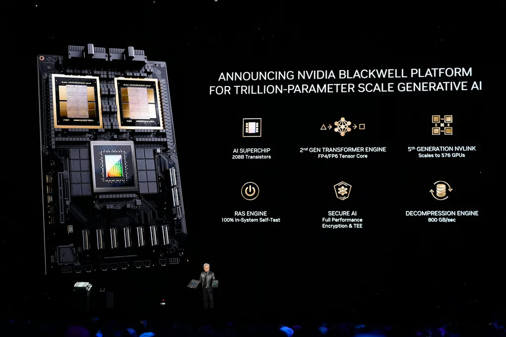
Blackwell B300: Performance and Technical Specifications
In comparing the B200 to the anticipated B300, the key focus stays on throughput and memory bandwidth. The B200 already set a high standard with its HBM3e integration, while the B300’s rumored 288GB capacity aims to tackle the bottleneck of model parallelism. For more details, check out OpenAI Blog.
We’re closely monitoring the production node; while the B200 used TSMC’s 4NP process, it looks like the B300 might use an updated version of this node to handle thermal issues and deliver better performance.
The table below summarizes the main differences between the established B200 and the expected B300 specifications based on the latest industry data.
| Feature | NVIDIA B200 (Confirmed) | NVIDIA B300 (Unconfirmed) |
|---|---|---|
| Memory Capacity | 192GB HBM3e | 288GB HBM3e |
| Production Node | TSMC 4NP | Updated 4NP Variant |
| Architecture | Blackwell | Blackwell |
Blackwell B300: Strategic Implications for AI Infrastructure
The shift to the B300 series underscores NVIDIA’s ambitious strategy to stay ahead of competitors like AMD EPYC in the NVIDIA hardware ecosystem. By enhancing the Blackwell architecture, the company aims to offer a smoother upgrade path for data centers already optimized for the B200. The pressing question is how quickly these units can reach hyperscalers, considering the complexities of high-bandwidth memory supply chains. For more information, visit VentureBeat AI.
While the start of B300 chip mass production is a notable industry milestone, the broader availability of these systems will shape the pace of AI development for the rest of 2026.
If the performance gains hit the projected 1.5 exaflops for the full rack systems, we can expect a rapid shift in procurement priorities among major cloud providers. However, we recommend caution regarding the unconfirmed pricing, as the added memory density will likely push these chips to be more expensive than their predecessors.
FAQs
When did NVIDIA officially announce the Blackwell architecture?
NVIDIA officially announced the Blackwell architecture at the GTC 2024 conference on March 18, 2024, in San Jose, California.
What’s the primary difference between the B200 and the rumored B300?
The main difference is memory capacity; the B200 has 192GB of HBM3e memory, while the B300 reportedly features 288GB of HBM3e memory, giving a significant boost for large-scale AI training.
Is the B300 production status officially confirmed?
As of June 12, 2026, various sources like The Information and DigiTimes have reported on mass production for the B300, but NVIDIA hasn’t released an official statement to confirm these timelines.
The industry is now looking forward to the initial wave of hardware deployments, which will show whether the B300 can effectively bridge the compute gap for next-generation generative AI agents. Blackwell B300


