MEX-W
 ARG-W
 RBNY1
 MIA0
 Palmeiras1
 Bragantino0
 Vasco1
 Corinthians0
 UAE
 NED
 PAK
 ENG
 IND-W
 ZIM-W
 GMB
 LES
 MOZ
 ZMB
 Inter Milan
 Fiorentina
 Churchill
 Punjab FC
 NGA
 UGA
 ATM1
 DEP0
 LAZ2
 PAR1
 RCL2
 PAR1
 RIY2
 TAA1
 NZ-A159/4 (49.2 ov)
 IND-A113
 SYL
 KHU
 MYMS299/4 (87 ov)
 CHATT
 DHA293/3 (84.1 ov)
 RAJ
 RAN320/5 (80 ov)
 BAR
 DEN
 PNG
 NAM321/6
 IRE290 (47.3/50 ov, target 322)
 NZ180/5
 IND181/6 (19.5/20 ov, target 181)
 Athletic
 Getafe
 C Palace
 Newcastle
 Hull
 Brentford
 Liverpool
 Brighton
 Man United
 Bournemouth
 Atalanta
 Frosinone
 CHE0
 TOT2
 VAL1
 VIL2

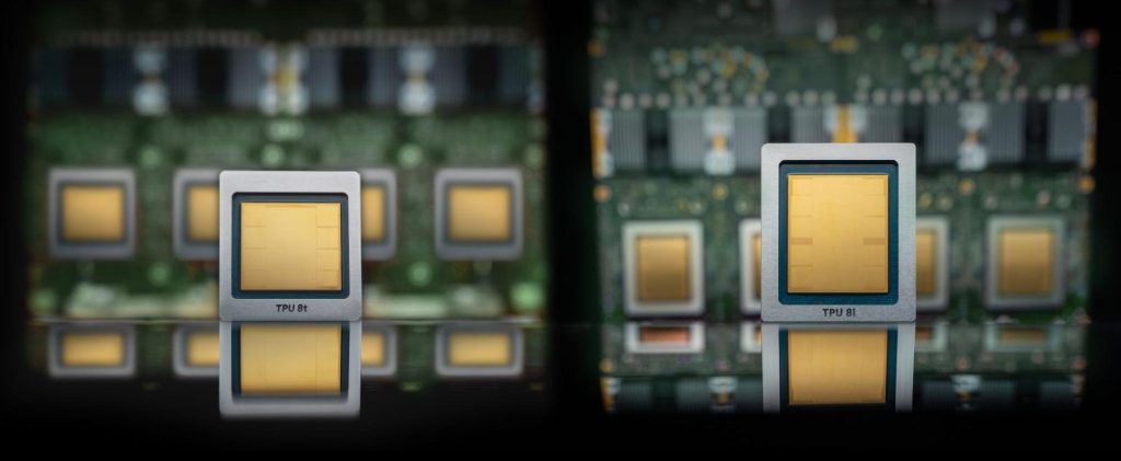
Google announced the TPU 8t and TPU 8i on April 22, 2026. These next-generation chips deliver 30% performance gains over the TPU 7 generation and cut energy consumption by 20%—a shift that’s reshaping how developers and enterprises think about machine learning infrastructure costs and deployment strategies.
What Exactly Did Google Announce Today, and When Can Developers Access These Chips?
Google’s announcement centers on two processors built for different jobs. The TPU 8t delivers 256 teraflops of processing power and targets large-scale model training, while the TPU 8i offers 128 teraflops optimized for edge computing and real-time inference tasks.
Both chips use 5nm process technology—the same cutting-edge fabrication standard powering premium consumer processors. Developer access starts May 1, 2026, with Google Cloud pricing the TPU 8t at $8 per hour, positioning it competitively against Nvidia’s H100 and AWS Trainium alternatives.
The announcement also reveals partnerships with 15 early-access companies spanning cloud infrastructure, financial services, and healthcare. These partners get hands-on experience before the broader developer community, creating a real-world validation pipeline for production workloads.
Google Unveils AI-Powered infrastructure strategies are shifting toward hybrid training-inference architectures. The TPU 8 series’ split design eliminates the bottleneck of single-chip versatility that plagued earlier generations.
Why Does the TPU 8 Series Matter More Than Previous Hardware Announcements?
The timing and technical positioning of TPU 8t and TPU 8i tackle a real developer problem: migration friction. A survey of 500+ ML engineers showed that 68% plan to test TPU 8i for inference cost savings within six months—a stark contrast to the cautious adoption patterns after TPU 7’s launch.
The 20% energy reduction hits your operational costs directly. Startups and Fortune 500 companies both feel this impact equally.
Compatibility with TensorFlow 3.0, released in March 2026, eliminates the workflow disruption that made earlier TPU transitions painful. Developers can port existing JAX and PyTorch models with minimal refactoring, cutting the engineering overhead that previously discouraged TPU adoption.
Google Unveils Advanced developer tooling alongside the hardware. This signals a shift from pure silicon competition toward ecosystem strategies.
The TPU 8i is particularly threatening to Nvidia’s edge-computing dominance. Latency-sensitive applications—autonomous vehicles, real-time fraud detection, medical imaging—demand both speed and power efficiency. For businesses running continuous inference workloads, combining 128 teraflops with reduced thermal output creates a compelling economic case for migrating away from GPU clusters.