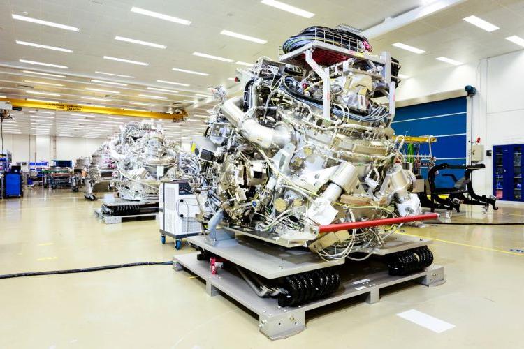
According to UDN, Huawei has filed a patent application for an extreme ultraviolet (EUV) lithography scanner. If the company can create such a scanner while maintaining reasonable productivity, uptime, and yields, Chinese chipmakers may be able to produce semiconductors on sub-7nm-class technologies.
Huawei filed a patent application with the State Intellectual Property Office in mid-November for an EUV scanner and its core components. According to MyDrivers, the patent application number is 202110524685X.
According to descriptions published by various media sources, the patent application appears to cover all critical components of an EUV scanner, including a 13.5 nm EUV light generator (light source), a set of reflecting mirrors, the lithography system, and ‘control management technologies’.
Filing a patent does not imply being able to build an EUV scanner, which is a highly complex system with several cutting-edge components that must perform flawlessly in tandem and for extended periods of time. Furthermore, even with an EUV tool at their disposal, chipmakers must still determine the proper pellicles for masks, resists, and a variety of other high-volume manufacturing requirements.
A 0.33 numerical aperture EUV scanner is the apex of today’s semiconductor production tools.

Many firms attempted to create such a tool, but only ASML succeeded after more than ten years of development and financial support from Intel, Samsung, and TSMC. Currently, Samsung, SK Hynix, and TSMC actively use ASML EUV tools, but Intel has yet to begin high-volume chip production using these tools.
For the time being, only Intel, Micron, Samsung, SK Hynix, and TSMC employ or plan to use EUV scanners. Furthermore, only these five companies have created (or plan to develop) sophisticated enough process technologies to take use of EUV scanners. Meanwhile, due to the Wassenaar agreement, China-based SMIC was unable to get an already purchased EUV tool to create its own EUV-based fabrication process. As a result, it is clear that demand for EUV scanners exists in China, and Huawei appears to be keen to meet it.
Huawei, a world-class high-tech firm with approximately $100 billion in yearly revenue, pursues several aims and develops numerous technologies. The company’s semiconductor production goals are widely known, and they extend beyond chip fabrication to the construction of wafer fab equipment. Huawei’s WFE efforts are doing nicely, as the company has submitted for a patent covering an EUV scanner.
Also Read:


