Samsung never specified what kind of components were produced on its cutting-edge node when it stated earlier this year that it had begun volume manufacturing of circuits using its 3GAE (3nm-class, gate-all-around early) process technology.
Apparently, Samsung fabricates an application-specific integrated circuit (ASIC) for cryptocurrency mining with the aid of 3GAE.
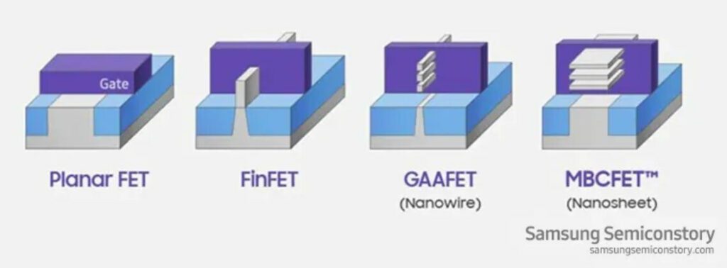
The industry’s first process to use gate-all-around (GAA) transistors, or what Samsung refers to as MBCFETs, is Samsung’s 3GAE fabrication technique (multi-bridge channel field-effect transistors). GAA transistor architecture allows for change of transistor performance and power consumption by modifying the channel’s thickness, which also minimises leakage current because the gate is now encircled by the channel across all four sides (s). Because GAAFETs are particularly advantageous for high-performance and mobile applications, businesses like Intel and TSMC are putting a lot of effort on utilising them in 2024 to 2025.
However, according to TrendForce, it appears that the first commercial chip to use GAAFETs is an ASIC for cryptocurrency mining. According to TrendForce analysts, the company won’t start manufacturing mobile system-on-chips utilising the 3GAE fabrication technique until the following year.
Due to their relative simplicity, small size, and abundance of comparable units and structures that may be employed for redundancy to achieve acceptable yields, cryptocurrency mining chips provide effective pipe cleaning vehicles for new manufacturing technologies. Mobile SoCs, in contrast, combine numerous wholly unique components that employ various transistor architectures, making it hard to construct redundant components. Nevertheless, it makes sense that Samsung would deploy crypto-mining ASICs to gather more information regarding the functionality, power, and fault density of its 3GAE node. As a result, SMIC tested their 7nm-class node using a MinerVa mining ASIC.
When it comes to brand-new nodes, Samsung typically has an advantage over TSMC and Intel, although in many circumstances, TSMC’s chips are faster and have greater yields. Maybe the organisation sets overly ambitious targets that can’t be met all at once. However, it appears that Samsung’s 3GAE is capable of producing bitcoin mining ASICs, with mobile SoCs occasionally following.
Also Read:
Intel accepts the leak of its Alder Lake UEFI BIOS
AMD Ryzen 7000 iGPU is offering a 20% performance increase with 3 GHz using MSI BIOS