Apple secures 50%+ capacity, AMD leapfrogs with Zen 6, Intel explores N2 for products—Q3 2026 revenue to surpass 3nm + 5nm combined as GAA architecture redefines chip economics.
TSMC’s 2nm gamble is paying off spectacularly. TSMC’s 2nm node has witnessed 1.5 times the number of tape-outs compared to the 3nm technology, indicating just how ravenous the demand is, according to JPMorgan analyst reports shared by industry tipster @jukan05.
The surge—driven by simultaneous adoption from mobile giants (Apple), HPC leaders (NVIDIA, AMD), and AI accelerator makers—marks the first time a leading-edge node has achieved faster customer onboarding than its predecessor, defying semiconductor industry norms where adoption typically slows at advanced nodes due to cost/complexity barriers.
Table of Contents
1.5x Tape-Out Surge: What the Numbers Mean
Reports indicate that the N2 family has recorded 1.5 times more “tape-outs”—the final stage of the design process before manufacturing—than the 3nm node did at the same point in its lifecycle. Tape-out represents the moment a chip design finalizes and heads to manufacturing—effectively a customer commitment to volume production. The 50% increase signals that more companies are betting bigger, earlier on 2nm than they did on 3nm, according to semiconductor manufacturing cycles.
Notably, strong demand from AI-related customers has driven a higher number of 2nm tapeouts in the first two years compared to 3nm and 5nm during the same period. This AI-driven acceleration explains why TSMC’s 2nm is bucking historical trends where each node generation saw slower adoption due to diminishing returns and exponentially rising costs.

Revenue Dominance: Surpassing 3nm + 5nm Combined by Q3 2026
TSMC’s 2nm revenue is reported to surpass the combined revenue of the 3nm and 5nm processes by the third quarter of 2026, making it another indicator of just how rapidly the technology is being adopted. This milestone—achievable just 12-18 months after mass production launch—represents the fastest node revenue ramp in TSMC history.
Each 2nm wafer could be priced as high as USD 30,000, representing a 50 percent increase over 3nm wafer pricing. At $30,000/wafer (vs $20,000 for 3nm), TSMC’s 2nm economics deliver 50% higher average selling prices (ASPs) while customer demand remains inelastic—proof that performance gains (18% faster or 36% lower power vs N3E) justify premium pricing in AI/HPC applications where every watt and millisecond matters.
Capacity Explosion: 140,000 Wafers/Month by End 2026
TSMC aims to reach 140,000 wafers by the end of 2026. What is impressive about this feat is that the 2nm process is expected to reach this number after just one year of officially entering mass production, nearly matching the 3nm’s maximum production limit of 160,000 wafers.
The production ramp trajectory:
- Q2 2025: 35,000 wafers/month (initial ramp)
- End 2025: 60,000 wafers/month (four fabs operational)
- End 2026: 140,000 wafers/month (matching 3nm’s peak in one-third the time)
TSMC aims to meet the high demand through the construction of three additional facilities in Taiwan, which is an undertaking that’s estimated to cost a whopping $28.6 billion. This represents TSMC’s largest single-node investment ever—dwarfing the $20 billion Arizona fab buildout and signalling the company views 2nm as a decade-defining technology rather than a transitional node.
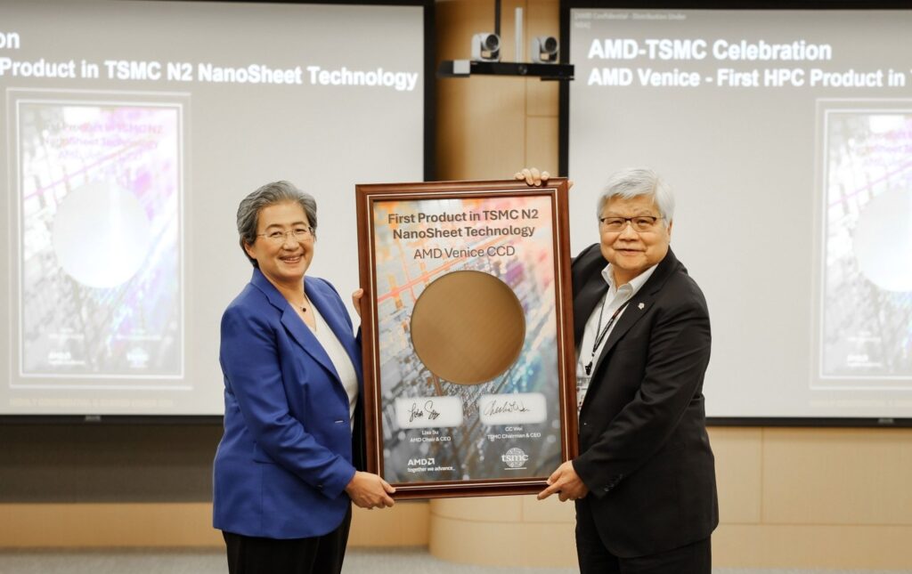
Apple Secures 50%+, AMD/Intel Join the Party
Apple, which was TSMC’s biggest customer in 2024, is said to have secured more than half of the initial capacity, with the majority of wafers likely being utilized for the A20 and A20 Pro, which will power the iPhone 18 series, followed by the M6 that’s expected to be incorporated in the OLED MacBook Pro.
Key customer commitments:
- Apple: A20/A20 Pro (iPhone 18), M6 (MacBook Pro 2026)
- AMD: Zen 6 CPUs, Instinct MI400 AI accelerators (announced at CES 2026)
- NVIDIA: Post-Blackwell “Rubin Ultra” AI GPUs
- MediaTek: Dimensity 9600 flagship SoC (taped out, mass production end-2026)
- Qualcomm: Snapdragon 8 Elite Gen 6 (rumored N2P variant)
- Intel: Nova Lake CPUs exploring N2 (hedging against 18A delays)
Even Intel, which was previously reported to leverage its 18A technology for the Panther Lake Core Ultra Series 3, is also said to explore TSMC’s N2 process for a number of products. Intel’s foundry struggles—18A yields reportedly trailing TSMC’s 70%+ 2nm yields—force the company to dual-source critical products, undermining CEO Pat Gelsinger’s “internal foundry first” mandate.
GAA Architecture: The Technical Revolution
The transition to the N2 node represents the most significant architectural change in chip manufacturing in over a decade. By moving from FinFET to GAAFET (Gate-All-Around Field-Effect Transistor) nanosheet technology, TSMC has effectively re-engineered how electrons flow through a chip.
GAA advantages over FinFET:
- Four-sided gate control (vs three-sided FinFET) eliminates current leakage
- Superior electrostatic control enables lower voltage operation
- Nanosheet flexibility allows tuning transistor width per function (high-performance vs low-power cores)
- Backside power delivery (N2P variant) separates power/signal routing, reducing resistance
Compared to the existing N3E process, TSMC’s enhanced 2nm process technology increases logic density by 1.2 times, improves performance by up to 18% at the same power consumption, and reduces power consumption by approximately 36% at the same speed.
95% AI Accelerator Market Share Projection
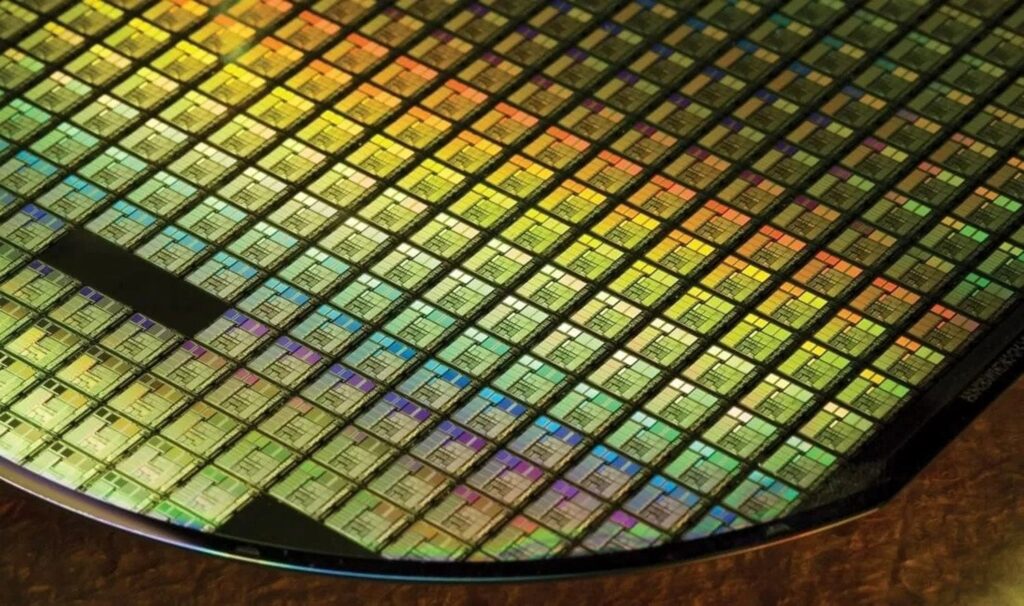
The unprecedented demand for TSMC’s 2nm node will allow it to obtain an impressive 95 percent market share in the AI accelerator market. This near-monopoly stems from:
- Samsung’s yield struggles: 50-60% yields (vs TSMC’s 70%+) double effective costs
- Intel 18A delays: Originally targeting 2024, now pushing 2026-2027 volume production
- Design ecosystem maturity: TSMC’s EDA tool partnerships reduce time-to-tape-out vs competitors
For AI companies like NVIDIA, AMD, and Google (TPU), TSMC’s 2nm becomes the only viable option for 2026-2027 product cycles—creating structural lock-in that could last through 2028 when competitors stabilize advanced GAA processes.
The $28.6 Billion Bet: 10 Fabs by 2028
TSMC could have as many as ten 2nm plants established on its home turf and in the United States, but it apparently has no plans to bring this technology overseas, and is said to arrive with the 3nm node instead, a year ahead of schedule. The geographic strategy:
- Taiwan (primary): Fab 22 (Kaohsiung), Fab 20 (Hsinchu), plus 5-6 additional facilities
- United States (delayed): Arizona fab prioritizes 3nm (2026), 2nm pushed to 2028+
- Europe/Japan: No 2nm plans; partnerships focus on mature nodes (28nm, 16nm)
The Taiwan concentration creates geopolitical risk—80%+ of cutting-edge chips manufactured within 100 miles of mainland China—but TSMC prioritizes technical execution over geographic diversification, betting that performance leadership trumps supply chain resilience concerns.
What This Means for Tech in 2026-2027
Smartphone revolution: iPhone 18 (A20 Pro), Galaxy S27 (potential Snapdragon N2), and Pixel 11 (Google Tensor G6 on N2) will deliver 30-40% battery life improvements or 2x AI performance without size/weight increases.
AI training costs plummet: 36% power reduction at same performance means data centers can train larger models (200B+ parameters) without upgrading electrical infrastructure—critical as power constraints limit AI scaling.
PC performance leap: Apple’s M6, AMD’s Zen 6, and Intel’s Nova Lake (if N2-based) will bring desktop-class performance to ultraportable laptops weighing under 1kg—redefining mobile workstation capabilities.
The tape-out surge isn’t hype—it’s capital allocation by the world’s largest tech companies betting $28.6 billion that 2nm defines the next computing era.
Also Read: AMD Zen 6 Architecture Deep Dive | Apple A20 Pro Performance Projections