The Taiwanese silicon giant has made a breakthrough in developing the finest silicon process nodes for its widest range of clients including AMD, Qualcomm, NVIDIA, MediaTek and others. So, from developing the 7nm process or delivering the newer 5nm process, TSMC has been ruling with its highly efficient and powerful silicon nodes.
TSMC is currently working on 2nm process and as Gizchina reports, as per the Taiwan Economic Daily the Taiwan giant’s research and development has made a major breakthrough in developing 2nm nodes. The company remains optimistic that its risk trial production yield in the second half of 2023 could actually reach 90%.
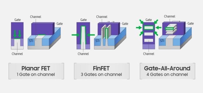
Interestingly, TSMC will be discarding the mostly-used FinFET process to adopt the new multi-bridge channel field effect transistor (MBCFET) architecture based on the surround gate (GAA) process. This helps to solve the physical limit of the FinFET’s current control leakage due to process shrinkage, helping to stuff more transistors in a small area.
The GAA (Gate-all-around, around the gate) process adopted by TSMC is not their sole weapon as Samsung too will implement this process but on the 3nm process. The GAA technology introduced by Samsung is Multi-Bridge Channel FET (MBCFET), which is actually a multi-channel bridge fin with a plate-like structure.
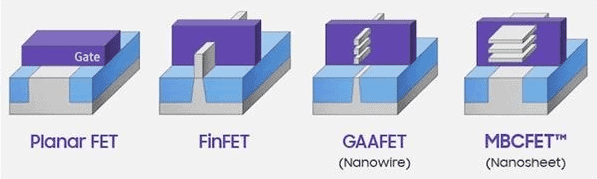
The GAA process also has different forms and the current four mainstream technologies are – nanowires, sheet-like structure multi-way bridging fins, hexagonal cross-section nanowires, and nanorings. Each has its own advanatages, while GAA can really help reduce power consumption while maintaining performance gains.
However, the cost of implementing GAA is also very high and the cost of the 28nm process used to cost $62.9 million, while the newer 5nm process surged to $476 million. Samsung even claims that the cost of its own 3nm process based GAA may exceed the $500 million mark.
Do check out: