Samsung‘s struggling 4nm foundry process has achieved 60-70% yield rates—a dramatic recovery from earlier 35% yields that drove Qualcomm to TSMC. This improvement secured a $100 million+ order from U.S. AI startup Tsavorite Scalable Intelligence to manufacture Omni Processing Units combining CPU, GPU, and memory.
Table of Contents
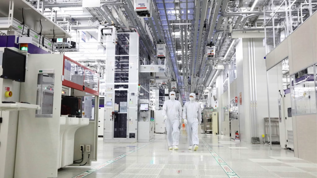
Samsung 4nm Process Recovery
| Metric | Previous | Current |
|---|---|---|
| 4nm Yields | 35% (2022) | 60-70% (2025) |
| Major Order | Lost Qualcomm | $100M+ Tsavorite OPU |
| Process Node | SF4X (4th gen) | Mass production active |
| Chipset Impact | Snapdragon 8 Gen 1 failure | Now competitive |
| Recent Wins | Tesla $16.5B, crypto miners | Chinese manufacturers |
| 2nm Status | 50-60% yields | Early production |
Omni Processing Unit Deal Details
Tsavorite Scalable Intelligence pre-ordered approximately 150 billion won ($100 million+) in AI chips using Samsung’s SF4X platform—the fourth-generation 4nm process. The Omni Processing Unit (OPU) integrates CPU, GPU, and memory on a single die, targeting cost-effective AI workflow scaling for Fortune 500 firms and sovereign cloud providers.
The deal leverages Samsung’s older 4nm node while 3nm and 2nm processes attract premium pricing. As documented in semiconductor manufacturing economics, mature nodes offer significant cost advantages for AI startups prioritizing volume over cutting-edge performance.
Samsung’s Foundry Comeback Timeline
Samsung’s 4nm journey illustrates foundry volatility. The Snapdragon 8 Gen 1 disaster—with only 35% usable chips per wafer versus TSMC’s 70%—drove Qualcomm to manufacture subsequent generations exclusively with TSMC. Poor thermal efficiency and power consumption became industry cautionary tales.
However, SF4X introduces Back-End-of-Line (BEOL) wiring technology improving power efficiency and performance, alongside higher-drivability transistors reducing RC delay. These refinements position Samsung competitively for HPC applications requiring mature process stability over density maximization.
Broader Foundry Recovery Signals
Beyond 4nm, Samsung secured orders from Chinese cryptocurrency mining equipment manufacturers and forged a $16.5 billion deal with Tesla—suggesting multi-node competitiveness. The company’s 2nm GAA Exynos 2600, while achieving only 50-60% yields in early production, represents progress toward advanced node manufacturing parity.
Industry observers note TSMC’s focus on mega-clients like NVIDIA and Apple creates opportunities for Samsung to capture specialized AI startups and mid-tier customers—a strategic pivot from direct flagship chip competition.
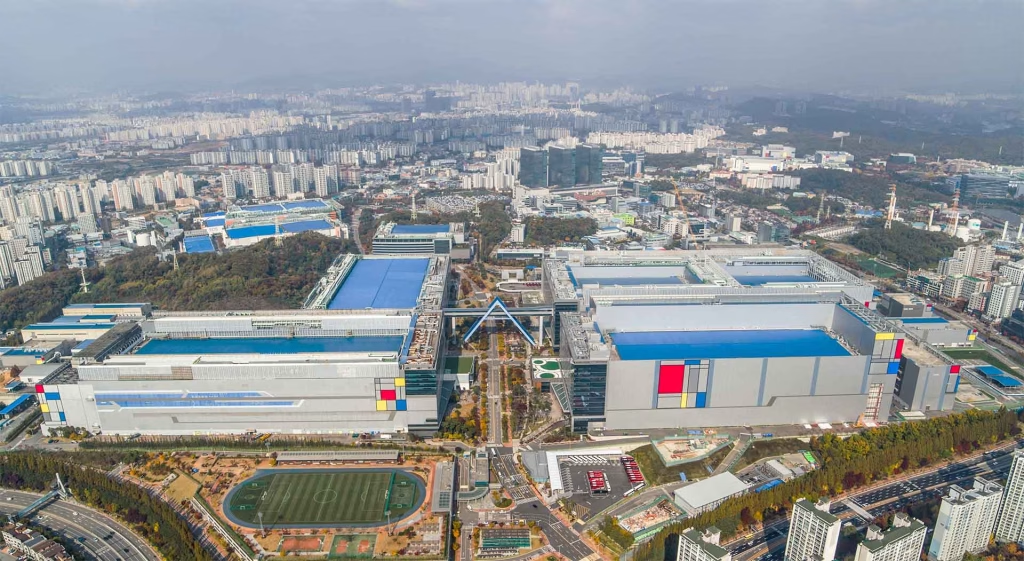
Why Yield Improvements Matter
Manufacturing yields directly impact profitability. At 35% yields, Samsung lost money on most wafers. At 60-70%, the economics flip positive, enabling competitive pricing against TSMC while maintaining margins.
For AI chipmakers like Tsavorite, Samsung’s improved 4nm yields offer established process reliability at discounted rates compared to bleeding-edge nodes—ideal for startups requiring predictable costs and supply chain diversification away from TSMC dominance.