TechnoSports Media Group
  • Home
  • Technology
  • Smartphones
  • Deal
  • Sports
  • Reviews
  • Gaming
  • Entertainment
No Result
View All Result
  • Home
  • Technology
  • Smartphones
  • Deal
  • Sports
  • Reviews
  • Gaming
  • Entertainment
No Result
View All Result
TechnoSports Media Group
No Result
View All Result

Samsung plans on displaying the potential of its Next-Generation 3nm Chip Technology to U.S. President Joe Biden This Week

Nivedita Bangari by Nivedita Bangari
May 20, 2022
in News, Technology
1

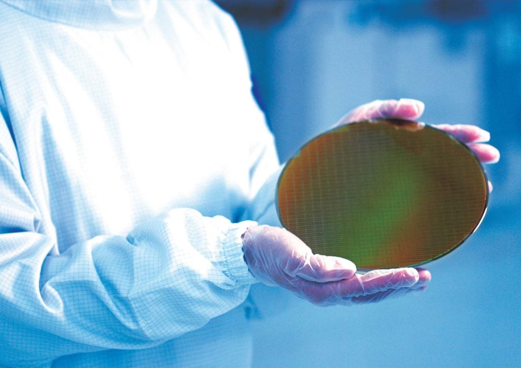
Samsung is scheduled to demonstrate its next-generation technology to US President Joe Biden when he visits the Korean giant’s Pyeongtaek campus this week, with its 3nm GAA process expected to begin commercial production soon.

 Samsung
credit:source


According to Yonhap, US President Joe Biden will arrive in Seoul for a three-day visit, which will include a tour of Samsung’s Pyeongtaek factory, which is also the world’s largest and is located 70 kilometers south of Seoul. Samsung’s Vice Chairman Lee Jae-Yong is expected to join Biden on the tour to demonstrate the next-generation mass production process.

RelatedPosts

Cognizant Adopts Anthropic’s Claude: 350,000 Employees to Drive AI Transformation

Unix introduces two vintage car-shaped Bluetooth speakers – Capri 52 and Pontiac 34

Canada’s Student Visa Crisis: 74% of Indian Applications Rejected in 2025

Samsung has been rumored to be starting mass production of its 3nm Gate-All-Around (GAA) technology for several months, surpassing Qualcomm’s 4nm node, which was used to mass create the Snapdragon 8 Gen 1. According to one official with knowledge of Samsung’s superior semiconductor production technology, the Korean behemoth’s objective is as follows.

“Samsung could show a 3-nm chip to Biden to emphasize its foundry prowess over Taiwan’s TSMC.”

 Samsung
credit:source

The benefits of 3nm GAA over Samsung’s 5nm process are significant, according to the company, with up to a 35 percent reduction in size, 30 percent higher performance, and 50 percent power savings. This 3nm GAA technique is most likely intended to compete with TSMC’s 3nm node, but the Taiwanese firm has long dominated the worldwide foundry industry.

TSMC captured 52.1 percent of the global foundry market in the fourth quarter of 2021, while Samsung, in second place, trailed far behind with only 18.3 percent 

According to a recent source, the Korean firm was having trouble manufacturing its 3nm GAA process, which had a lower yield rate than its 4nm technology. If Samsung cannot enhance these yields while simultaneously demonstrating that its 3nm GAA process is competitive with TSMC’s 3nm wafers, it may be unable to get orders from Qualcomm and others. Samsung is slated to begin mass production of its advanced chip technology shortly, so we’ll see how it compares to what TSMC has to offer.

also read:

Honor MagicBook 14 2022 launches with Intel’s Alder Lake

source

Tags: SamsungTSMC
Previous Post

PSG offer Kylian Mbappe insane contract worth £4m per month and to become the owner of their Sporting Project to get him to stay

Next Post

Sony LinkBuds S launched as the ‘smallest & lightest’ ANC earbuds

Related Posts

Cognizant Adopts Anthropic's Claude
Recent News

Cognizant Adopts Anthropic’s Claude: 350,000 Employees to Drive AI Transformation

November 4, 2025
Unix introduces two vintage car-shaped Bluetooth speakers - Capri 52 and Pontiac 34
Technology

Unix introduces two vintage car-shaped Bluetooth speakers – Capri 52 and Pontiac 34

November 4, 2025
Canada
News

Canada’s Student Visa Crisis: 74% of Indian Applications Rejected in 2025

November 4, 2025
Trrssa
FAQ

Trisha Kar Madhu’s Boyfriend MMS Leak: The Controversy, His Response, and What It Means?

November 4, 2025
Sona Dey Speaks Out: Viral MMS Controversy and the Perils of Digital Manipulation
Entertainment

Sona Dey Speaks Out on the Viral MMS Controversy as of 2025

November 4, 2025
Entertainment

Kajal Raghwani MMS: The Truth Behind the Viral Video as of 2025

November 4, 2025
Next Post
Sony LinkBuds S

Sony LinkBuds S launched as the 'smallest & lightest' ANC earbuds

Comments 1

  1. Avatar of Daniel Daniel says:
    3 years ago

    Samsung 3nm yields are still in the 20% range, and anything Samsung claims to the contrary, are lies, by their own admission. They have repeatedly and continuously lied about their 5nm, 4nm, and 3nm yields, and after recently getting caught lying, admitted they were lying, and now suddenly we are supposed to believe they have miraculously improved yields.

    TSMC doesn’t start production until yields are around 70%, and shortly after production mature yields are around 90%.

    The truth will be revealed soon enough, when both Samsung and Intel are forced to admit that their latest and most overly-promised nodes are late, and then late again, and for the 3rd time late again, and ….

    Reply

Leave a Reply Cancel reply

Your email address will not be published. Required fields are marked *

This site uses Akismet to reduce spam. Learn how your comment data is processed.

TechnoSports Media Group

© 2025 TechnoSports Media Group - The Ultimate News Destination

Email: admin@technosports.co.in

  • Terms of Use
  • Privacy Policy
  • About Us
  • Contact Us

Follow Us

No Result
View All Result
  • Home
  • Technology
  • Smartphones
  • Deal
  • Sports
  • Reviews
  • Gaming
  • Entertainment

© 2025 TechnoSports Media Group - The Ultimate News Destination