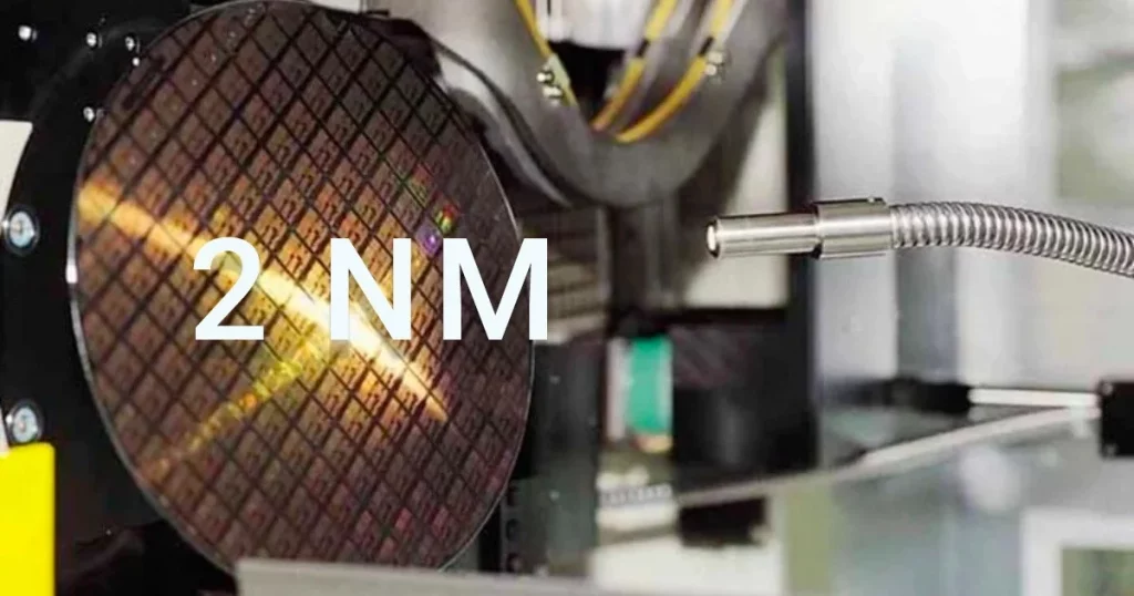
Japan will work with the U.S. to launch a domestic manufacturing base for 2-nanometer semiconductors as early as fiscal 2025, Nikkei has learned, joining the race for commercializing the next-generation chip technology.
Tokyo and Washington will provide support under a bilateral chip technology partnership. Private companies from the two countries will pursue research on design and mass production.
Taiwan Semiconductor Manufacturing Co. is ahead in developing mass production technology for 2-nm chips. Japan seeks to secure a stable supply of semiconductors by realizing domestic production of the next-generation chips.
Companies from Japan and the United States could merge to form a new corporation, or Japanese companies could create a new industrial cluster. The Japanese Ministry of Economy, Trade, and Industry will partially fund R&D and capital expenditures.
Joint research will commence this summer, and between fiscal years 2025 and 2027, a research and mass manufacturing plant will be constructed.
TSMC, the world’s largest contract chip manufacturer, is building a chip fab in Kumamoto, Japan, although it will only produce less-advanced semiconductors scaled from 10nm to 20nm
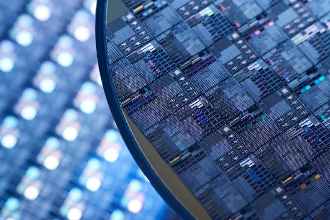
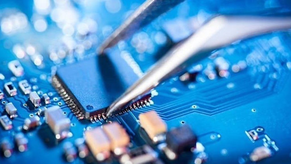
Smaller semiconductors enable miniaturization and improved device performance. The 2-nm circuits will aid quantum computers, data centers, and cutting-edge cellphones. These chips assist in cutting carbon emissions by reducing power use.
Depending on their size, military hardware such as fighter jets and missiles may perform differently. As a result, the security of 2-nm semiconductors is closely linked.
In early May, Japan and the United States signed basic principles for semiconductor cooperation. The two parties will debate the finer points of the cooperative framework during a planned “two-plus-two” meeting of cabinet economic officials.
The cabinet approved Prime Minister Fumio Kishida’s “new capitalism” plan last week, which calls for the construction of a design and manufacturing base in Japan this decade through a bilateral public-private partnership with the United States.
IBM, which specializes in 2-nm R&D, created a prototype last year. Intel, another American company, is also working on the 2-nm process.

At a research center in Tsukuba, Japan’s National Institute of Advanced Industrial Science and Technologies (NIST) is supporting a collaboration to develop manufacturing technologies for advanced semiconductor lines, including those for 2-nm processes. Chipmaking equipment manufacturers such as Tokyo Electron and Canon are included in the consortium, in addition to IBM, Intel, and TSMC.
In Japan, Shin-Etsu Chemical and Sumco manufacture high-quality chip materials, whereas Applied Materials is a chipmaking equipment powerhouse in the United States. The purpose of this partnership between chipmakers and key suppliers is to bring 2-nm device mass manufacturing closer to reality.
TSMC is at the forefront of mass-production of next-generation chips. After breaking ground on a 2-nm fabrication unit earlier this year, the company aims to begin large-scale manufacturing of 3-nm devices later this year.
also read:
AMD is rumored to launch its Radeon RX 7000 GPU Series in Late October and Mid-November 2022