The Intel Labs and Components Research divisions have shown silicon spin qubit devices created at Intel’s transistor research and development site, Gordon Moore Park in Ronler Acres in Hillsboro, Oregon, to have the best reported yield and uniformity in the industry to date. This accomplishment is a significant step in the scalability and development of the transistor manufacturing procedures used by Intel to fabricate quantum devices.
The second-generation silicon spin test chip from Intel was used in the study. The scientists extracted 12 quantum dots and four sensors while testing the gadgets using the Intel cryoprober, a quantum dot testing equipment that runs at cryogenic temperatures (1.7 Kelvin or -271.45 degrees Celsius). With a single electron at each place over the whole 300 millimetre silicon wafer, this result is the largest silicon electron spin device in the industry.
Contrary to how silicon spin qubits are normally presented, Intel’s research shows success throughout the course of an entire wafer.
The chips, which were created using EUV lithography, exhibit amazing uniformity with a 95% yield rate throughout the wafer. More than 900 single quantum dots and more than 400 double quantum dots at the last electron were described at one degree above absolute zero in less than 24 hours thanks to the employment of the cryoprober and reliable software automation.
Compared to earlier Intel test chips, devices defined at low temperatures have a higher yield and more consistency, which enables Intel to employ statistical process control to pinpoint parts of the fabrication process that could be improved. This quickens learning and is an important step in scaling up to the hundreds, or perhaps millions, of qubits needed for a practical quantum computer.
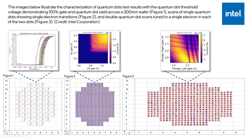
The greatest demonstration of single and double quantum dots to date was made possible by Intel’s ability to automate the collecting of data across the wafer at the single electron regime thanks to the cross-wafer yield. A significant step toward scaling to the hundreds or maybe millions of qubits needed for a commercial quantum computer is represented by this improved yield and uniformity in devices defined at low temperatures over prior Intel test chips.
Also Read: