Fujitsu, renowned as the largest IT services provider in Japan, often recognized even if its precise role is unclear to many, has established India as its primary research hub outside of Japan. During a recent visit to India, Fujitsu’s Chief Technology Officer, Vivek Mahajan, shared insights into the significant research and development efforts undertaken by Indian engineers for the company’s competitiveness across various cutting-edge technology domains.

2nm Chip Manufacturing at Fujitsu
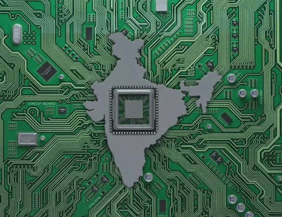
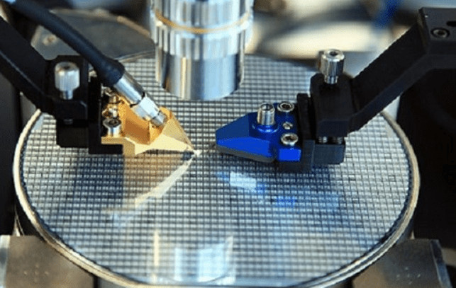
The Indian team is actively engaged in pioneering work on one of the world’s first 2-nanometer CPU chips, codenamed Fujitsu Monaka. Scheduled for release around 2027, Monaka is anticipated to find applications in high-performance computing (HPC), artificial intelligence (AI), and data center deployments. Fujitsu aims for Monaka to stand out as one of the most energy-efficient chips designed for high-end computing demands, an ever-growing requirement in today’s tech-driven world.
Notably, the software development for this groundbreaking and energy-efficient chip is taking place in India. Describing Monaka as an ARM-based 2nm processor with a strong focus on machine learning and deep learning workloads, Mahajan emphasizes its suitability for government entities and companies seeking power savings with an open architecture.
Fujitsu advocates for open architecture, a stance that adds complexity to the engineering work. According to Mahajan, Monaka necessitates open-source software, requiring compatibility with various packages to maximize performance. The team’s goal is to ensure seamless integration with the Monaka chipset, leveraging its capabilities to the fullest extent.
Highlighting the achievements in patent development, Mahajan acknowledges the excellence of Fujitsu’s India teams in creating proprietary technology. Among the five key technology domains the teams work on—AI, networking, data & security, computing, and converging technologies—computing stands out with the highest number of patents. Mahajan emphasizes the significant intellectual property Fujitsu holds in computing, exemplified by the Fugaku supercomputer.
Additionally, the company has a considerable patent portfolio in networking, particularly in optical communication technology. In converging technologies, the Indian teams hold a noteworthy number of design patents, specifically in screen designs that directly impact user experience.