
 SA329 (82.3 ov)
 AUS
 FLE1
 ARS1
 BAN
 WI
 IND-W
 ZIM-W
 GOA
 SC Delhi
 Milan
 Bologna
 Parma
 Udinese
 Venezia
 Inter Milan
 Genoa
 Juventus
 Monza
 Napoli
 ROMA4
 CAG2
 TOR1
 COMO3
 SAS2
 LAZ6
 AFG177
 ZIM140 (19.1/20 ov, target 178)
 AUCK
 CANT
 CD
 ND
 SIKM184
 NAGA187 & 46/4 (34 ov)
 JHK131/4 (47 ov)
 DELHI515/5d
 ODSA194
 SVCS13/0 (5 ov)
 BRODA616
 J & K6/0 (4 ov)
 CHD685/5d
 HP49/0 (14 ov)
 CGR216/8 (95 ov)
 AP231
 HYD193/2 (54 ov)
 PNJB431
 KNTKA297/7 (95 ov)
 TPURA194
 KER101/6 (35 ov)
 BENG350
 UAE
 OMA
 ENG
 SL
 DEN
 QAT
 KENYA
 KUW
 POA
 SPR
 BRB
 VAG
 PAK110
 NAM316/7
 IRE253 (44.5/50 ov, target 317)
 NZ198/3
 IND199/4 (13.2/20 ov, target 199)
 NED371/5
 JAB113 (19.3/20 ov, target 133)
 KAY132/9
 DON2
 EXT3
 MNR0
 AND2
 PEN1
 CLY1
 HUE1
 RAY1
 Gamba Osaka
 Buriram
 Kashima
 Pohang Steelers
 ABH0
 ALF1
 Sevilla2
 Osasuna0
 PSG2
 Lyon0
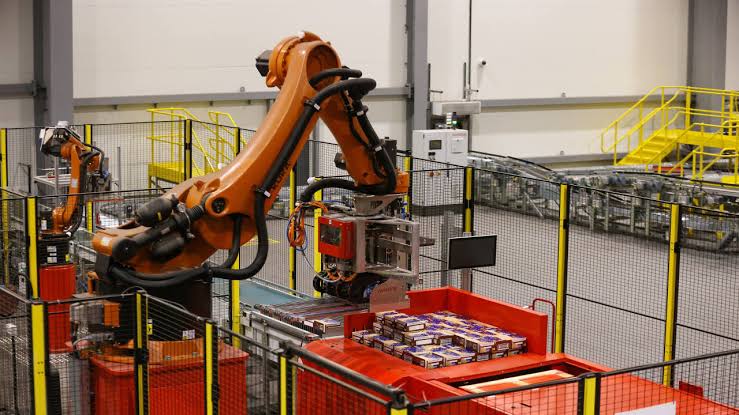
Chip Supply Chain Shift: Everyone says chip supply chains change slowly. The latest substrate packaging shift says otherwise. The hum of automated assembly lines in Shenzhen recently crossed a quiet threshold. Production yields stabilised while unit costs dropped sharply, marking a definitive turning point for next-generation semiconductor integration. This facility expansion signals a deliberate rebalancing in global hardware manufacturing priorities. According to 36kr, major component manufacturers are accele
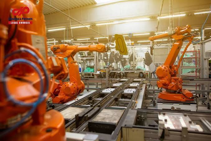
Production Scale And Yield Metrics
Early deployment phases revealed significant technical hurdles regarding signal integrity across densely packed circuit layers. Engineering teams responded by refining solder joint precision and adjusting micro-channel geometries within the package housing. These precise adjustments reduced defect rates substantially, allowing fabrication plants to scale operations without compromising long-term reliability standards.
Worth noting: the revised manufacturing protocols now support thicker interconnects and higher pin densities. This capability enables faster data transfer speeds between memory controllers and application processors. Suppliers report that the updated process architecture maintains consistent clock speeds even under sustained computational loads, eliminating previous throttling issues during heavy workloads. That said, industry analysts caution against assuming immediate cost reductions across all device categories. Premium segments benefit most from the refined substrate designs, while budget categories continue relying on legacy packaging methods. The technology migration remains gradual, requiring months of calibration before widespread adoption occurs across mid-range product lines.
Strategic Implications For Device Manufacturers
Original equipment makers now face tighter integration timelines when incorpo
Market Outlook And Future Developments
Analysts project continued refinement in packaging techniques throughout the remainder of 2026. As production volumes increase, economies of scale should gradually lower average component pricing for downstream assemblers. Device makers will likely pass these savings to consumers through more competitive retail positioning or enhanced feature bundles in upcoming generations.
We expect regional manufacturers to begin announcing hardware updates that leverage the improved substrate architecture. Early adopters will showcase devices featuring faster processing cores and more efficient power management systems. The broader ecosystem will eventually standardise around these new baseline specifications, raising the performance floor for entry-level offerings and forcing legacy competitors to accelerate their own innovation pipelines.
FAQs
How does the new substrate technology affect battery life?
The advanced packaging reduces electrical resistance between components, which directly lowers power consumption during intensive tasks and extends overall device runtime.
Will budget smartphones receive these upgrades immediately?
No, cost-sensitive manufacturers will likely continue using established packaging methods until the new technology achieves broader
What regions are driving this manufacturing shift?
Asian fabrication hubs are leading the transition due to concentrated expertise in high-density interconnect assembly and proximity to major consumer electronics markets.
How long until these changes impact everyday users?
Consumer devices incorposix to nine months after factory validation completes successfully.
Are there any downsides to the new production methods?
Initial setup costs remain high, and manufacturers must invest heavily in specialised inspection equipment to maintain strict quality control standards during the transition period. Source: 36kr.
Was this article helpful?
Your feedback directly improves future articles on this site.


