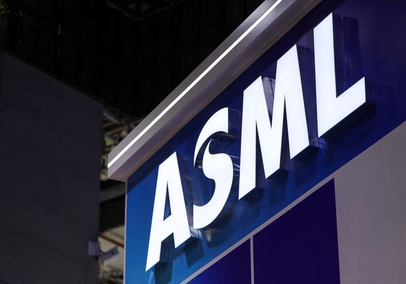
Dutch chipmaking equipment giant ASML just inaugurated its first American training center in Phoenix, Arizona. The 56,000-square-foot facility will train over 1,000 engineers annually on advanced EUV lithography machines, addressing America’s critical semiconductor talent shortage.
Table of Contents

ASML Arizona Facility: Key Details
| Information | Details |
|---|---|
| Location | Phoenix, Arizona (near airport) |
| Size | 56,000 square feet |
| Annual Capacity | 1,000+ engineers (expandable to 2,000) |
| Inauguration Date | November 20, 2025 |
| Classrooms | 14 modern classrooms |
| Equipment | DUV and EUV machines, cleanroom |
| Training Duration | 3-6 months (basic); longer (advanced) |
| Global Network | 9th training center worldwide |
Why This Matters for U.S. Semiconductors
Talent Gap Solution: American semiconductor expansion faces a critical shortage of engineers skilled in operating ASML’s complex lithography equipment. Previously, engineers traveled to Europe or Asia for training—a costly, time-consuming barrier now eliminated by this Phoenix location.
Supporting Regional Growth: The facility arrives perfectly timed with major investments by Intel, TSMC, and Samsung expanding Arizona and Texas fabs. CEO Christophe Fouquet noted Idaho and additional states will follow, creating unprecedented demand for trained engineers.
Military Recruitment Focus: ASML targets ex-military personnel, particularly former Navy and Air Force technicians experienced with F-35 fighter jets. VP Clayton Patch compares servicing EUV machines to maintaining advanced warplanes, making veterans ideal candidates.
Facility Features: Fourteen classrooms and a cleanroom provide hands-on experience with ASML’s DUV and EUV equipment. The facility operates 24/7 capability to meet growing demand, training both ASML staff and fab engineers from paying customers.
High-NA EUV Exception: The most advanced High-NA EUV tools—costing approximately $400 million each—still require Netherlands training. Intel and TSMC currently qualify these cutting-edge systems before high-volume production begins.

Economic Impact
Arizona Governor Katie Hobbs called the center “a major milestone for our state’s semiconductor workforce leadership”, while Phoenix Mayor Kate Gallego highlighted the city’s position as “the center of America’s semiconductor comeback.”
ASML employs about 700 people statewide in Arizona, with hundreds stationed inside semiconductor fabs operating lithography tools. This training facility strengthens America’s domestic chip supply chain resilience.
For more information, visit ASML’s official site or Arizona Commerce Authority. Stay updated at TechnoSports.