Moore’s Law is Dead has detailed AMD Instinct MI300 GPUs, which will be powered by the next-generation CDNA 3 architecture. The new GPUs, which are reported to be the first to integrate a 3D-Stacking design, will power the next data centers.
The top-of-the-line AMD Instinct MI300 GPU will have a huge interposer of roughly 2750 mm2. The interposer has a unique layout, with four 6nm tiles containing I/O controllers and IP Blocks that measure between 320 and 360mm2. These tiles are based on a 6nm node and may have a cache, however, this has yet to be confirmed. AMD will now use the brand-new 3D-Stacking technology to include two Compute Dies on top of these IO stacks.
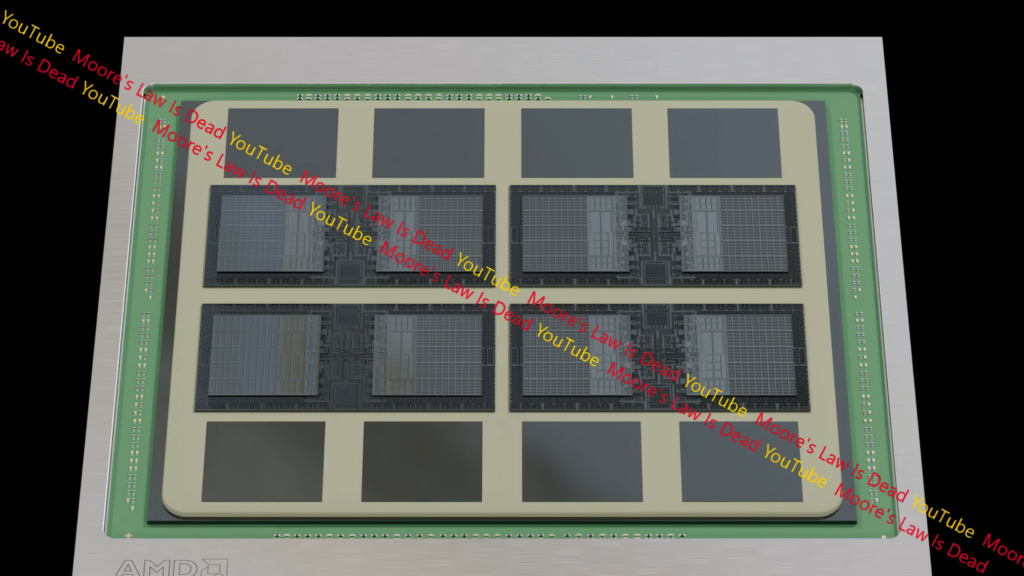
The new AMD CDNA 3 architecture-based Compute Dies will be manufactured on a 5nm node and have a die size of approximately 110mm2 per tile
There’s no mention of how many cores or accelerator blocks each Compute die will carry, but if we use the same SP/core count as the MI250X, we can obtain up to 28,160 cores, but this is just guesswork because so much can change in CDNA 3.
The memory controllers are connected to two stacks of HBM3 utilizing more than 12 metal layers because they are onboard the bottom I/O die. Each die is coupled by a total of 20,000 connections, which is twice as many as Apple uses in its UltraFusion chip design on the M1 Ultra.
While AMD is still using 8-stacks, they are now adopting the newer HBM3 standard, which is the same as NVIDIA’s Hopper GPUs. Currently, the MI250X employs 8 HBM2e stacks, each of which is 8-high and has 16 GB of memory (128 GB per module).
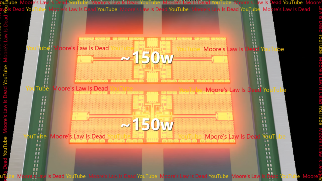
AMD may increase the stack height to 12-Hi, which SK Hynix has already hinted at. On the top Instinct MI300 GPU configuration, this would result in memory capacity of up to 192 GB, a 50 percent increase. The TDP of each cDNA 3 tile (1x 6nm + 2x 5nm dies) is expected to be roughly 150W.
The following are the possible configurations:
- Top Config: 4x IO Die (6nm) + 4x GCDs (5nm) + 8x Compute Dies (5nm)
- Mid Config: 2x IO Die (6nm) + 2x GCDs (5nm) + 4x Compute Dies (5nm)
- Low Config: 1x IO Die (6nm) + 1x GCDs (5nm) + 2x Compute Dies (5nm)
As a result, the top configuration will use roughly 600W of electricity, the middle configuration will use around 300W, and the entry-level configuration would use around 150W. The top Instinct MI250X configuration currently uses 560W and is available in the OAM form factor.
Next year, the Instinct MI300 GPUs will be released around the same time as Intel and NVIDIA’s latest data centers solutions, such as Ponte Vecchio and Hopper.
also read:
Karnataka might be inching closer to acquiring the ISMC deal