Recent reports out of Korea surfaced suggesting AMD and Samsung could be collaborating on Samsung’s 3-nanometer (nm) semiconductor manufacturing process technology – in a month full of rumors surrounding the semiconductor industry. Samsung and TSMC divide the world between them, serving companies such as AMD and NVIDIA that cannot afford to run their own chip-making lines. With smaller transistors at 3-nanometer nodes from each firm’s different transistor designs, TSMC remains committed to its trusted FinFET setup while targeting the use of nanosheet transistors in future processes.

More About AMD and Samsung Collaborating
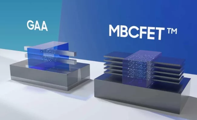
On the other hand, Samsung provides a way forward with its newer gate-all-around (GAAFET) transistors that can let chip designers improve how electricity flows through their devices – with some trade-offs.
Samsung is planning to improve its partnership with AMD and the two are expected to cooperate in producing 3 nanometer-based chips, as per a report from the Korea Economic Daily. Chips built with this technology are not available for most personal computers today, as only Apple’s Mac lineup features those produced by Taiwan Semiconductor Manufacturing Co Ltd (TSMC).
The highlight of Samsung’s 3-nanometer process is that it uses gate-all-around (GAAFET) transistors. GAAFET brings a new transistor design beyond FinFET, providing better electrical flow with a full gate wrapping around the transistor channel.
The GAAFET transistors guide current using nanowires or nanosheets, each with different trade-offs. Nanowires help to increase the area but since there the space is limited, they are restricted to some types of products such as application processors. Nanosheets, on the other hand, experience more loss in conduction efficiency but enable greater current flow.
Diagram of the evolution of transistors from FinFET to GAAFET and MBCFET by Samsung Foundry. Samsung’s 3-nanometer GAAFET transistors come from its joint development work with IBM.

During a recent conference in Belgium, AMD CEO Lisa Su apparently mentioned the benefits that can be reaped from relying on GAAFET transistors (over FinFET) and leaned towards configuring the pair for joint development. This technology is gate-all-around and Su also assured that they will… all mass-produced next-generation products of AMD using this new process.
The fact that Samsung will be the only 3-nanometer GAAFET provider in the world means Su could end up referring to Korea’s foundry, according to analysts. However, according to Su, 3-nanometer GAAFETs do provide performance and efficiency advantages relative to what had come before.
Samsung and Intel: Challenging TSMC in the contract semiconductor fabrication game With TSMC in the lead, its competition is catching up in many ways with new tech. Intel looks to High NA EUV lithography tools for chipmaking, and Samsung takes the lead on GAAFET transistors with a plan for an 8nm process before TSMC
Conversely, TSMC asserts its ability to use conventional EUV machines for chip production, with plans to transition to nanosheet transistors in its 2-nanometer process. Gate-all-around transistors represent a consequence of shrinking feature sizes, as manufacturers encounter challenges with FinFETs at smaller scales.
