Apple’s A17 processor marked the first chip to utilize TSMC’s N3 (3nm-class) process technology. This week, Apple extended its N3 lineup, introducing a series of PC-oriented M3 chips designed for desktop and laptop computers. According to analyst Jay Goldberg from Digits to Dollars, the company’s investment in the design and tape-outs of these M3 chips alone may have reached a staggering $1 billion.
All About Apple’s Investment in M3 Processor
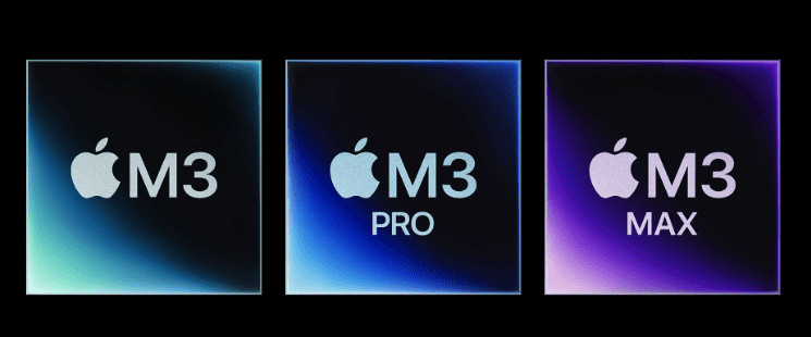
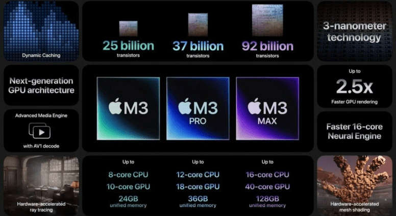
Apple’s M3 family comprises three sophisticated CPUs: the 25-billion-transistor M3 for entry-level and mainstream desktops, laptops, and high-end tablets; the 37-billion-transistor M3 Pro for performance-mainstream devices; and the M3 Max with a whopping 92 billion transistors for high-end laptops and entry-level workstations. Each chip is tailored to address various computing needs, from everyday tasks to professional coding, heavy engineering simulations, and video production.
Apple’s use of TSMC’s N3 fabrication process was a bold but calculated move to enhance the economic efficiency of its M3 family. As pointed out by chip analyst @Frederic_Orange, Apple could potentially fit around 415 M3 dies on a single 300-mm wafer, indicating a die size of approximately 146 mm^2. In comparison, AMD’s Phoenix, with similar complexity, boasts a larger die size of 178 mm^2. While it remains speculative whether Apple’s M3 is more cost-effective to produce than AMD’s Phoenix based on rumored TSMC quotes, smaller chips often exhibit better yield rates and cost efficiency.
The tech giant allocated a substantial portion of its $26.251 billion R&D budget in 2022 to chip design. The extensive investment in silicon and the M3-series SoCs underscores Apple’s financial capacity to undertake such ambitious development projects. Developing intricate PC-oriented processors necessitates long development cycles, typically spanning several years and substantial capital investments.

The base M3 chip, equipped with eight general-purpose cores and a new integrated GPU, rivals the complexity of AMD’s well-regarded Phoenix processor (25 billion vs. 25.4 billion transistors). In contrast, the M3 Pro and M3 Max are notably more intricate. The M3 Max, with 92 billion MOSFETs, stands as the most complex single-die processor to date, although this distinction may not hold for long considering upcoming AI processors.
When venturing into an entirely new platform like the M3 family, the development costs are monumental, particularly given Apple’s preference for internal IP development. With the M3, Apple not only employs its custom general-purpose cores based on the Arm instruction set architecture but also introduces a new GPU architecture supporting hardware-accelerated ray tracing and mesh shaders, a novel AI NPU, and a cutting-edge multimedia engine.