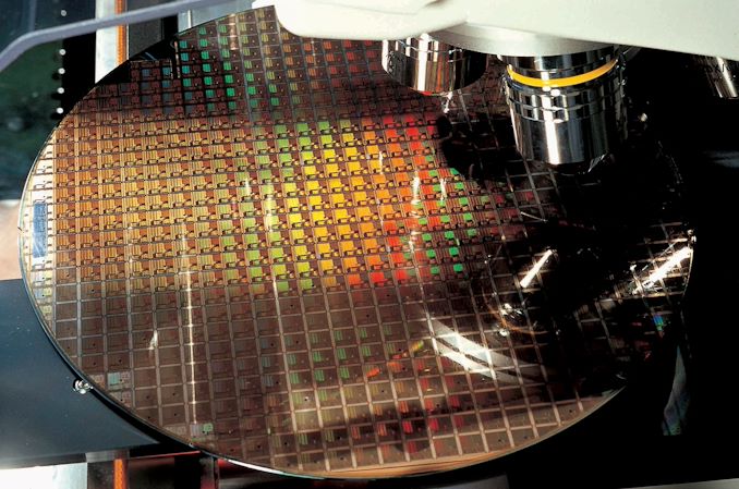
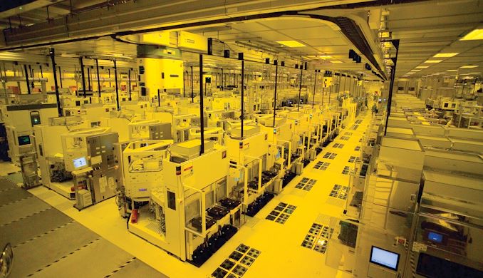
TSMC began mass production of chips based on its first N3 (3nm-class) fabrication process several months after Samsung Foundry began high-volume manufacturing using its 3GAE (3nm-class, gate-all-around early) node, but TSMC’s yields are significantly higher, according to a Business Next report citing various industry analysts and experts, but TSMC has not confirmed the reports.
Analysts and semiconductor specialists questioned by Business Next estimated that TSMC’s N3 yields may be as low as 60% to 70% or as high as 75% to 80% at the moment, which is fairly good for the first batch. Meanwhile, financial expert Dan Nystedt tweeted that TSMC’s current N3 yields are comparable to N5 yields early in the ramp-up, which might be as high as 80%, according to media reports.
According to the report, which cites industry sources without elaborating, Samsung Foundry’s 3GAE yields were from 10% to 20% in the early stages and have not improved. According to the research, the diversity in chip quality was also very high.

Given that TSMC develops its cutting-edge production technologies with Apple’s — its biggest customer and alpha client for cutting-edge nodes — requirements in mind, and that the Cupertino, California-based high-tech behemoth tailors its designs for TSMC’s capabilities, initial yields could be as high as 80%. Meanwhile, a yield rate of 60% may not be ideal for a chip (or chips) designed to power mass-market items.
In any case, because the number of N3 designs produced commercially by TSMC is limited for the time being, and yield-related data is a closely guarded trade secret of the foundry and its clients, we cannot make any judgements about how high or low TSMC’s N3 yields are.
It’s better to avoid comparing TSMC’s N3 yields to Samsung Foundry’s 3GAE yields in its early stages for the same reason.
Furthermore, given the rumours surrounding the first N3 node (called N3B), Apple may be the only firm to use this technology at all, as other developers are expected to use N3E, which has a better process window. Meanwhile, early N3 yields may not apply to N3E (and other nodes from its N3 technology family), and this process technology is something that the industry as a whole should be concerned about because it will be widely used.

Modern semiconductor manufacturing processes include thousands of process stages that are dependent on materials, fab equipment tools, process recipes, and a variety of other elements. As a result, there may be hundreds of methods to improve or decrease yields, which is why it is critical to have a thorough understanding of how one element affects others. Because TSMC’s N3 (N3B), N3E, N3S, N3P, and N3X production methods are so varied, early N3 yields are encouraging for the remainder, but they do not ensure that subsequent nodes will be as successful (or not as successful).
Also read:


