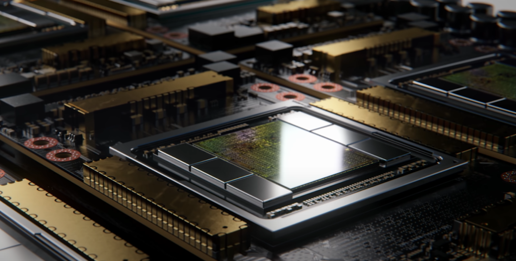
NVIDIA may be having difficulties obtaining a trademark for its next-generation Hopper GPUs, but that won’t stop the company from developing the flagship GH100 die, according to the newest rumour from Kopite7kimi, which claims that the chip will be approximately 1000mm2.
The NVIDIA Ampere GA100, which measures 826 mm2, is currently the largest GPU in production. If the story is true, NVIDIA’s Hopper GH100 will be the world’s largest GPU design, measuring over 1000mm2 and easily outstripping current monster GPUs by at least 100mm2.
But that’s not all; the die size in question is for a single GH100 GPU die, and we’ve heard that Hopper will be NVIDIA’s first MCM chip design, so if we receive at least two Hopper GH100 GPUs on the same interposer, the dies would be 2000mm2.
All of this implies that the interposer will be much larger than what we’ve seen so far, given that it will include numerous HBM2e stacks and additional connectivity. However, Greymon55 has claimed that Hopper would remain a monolithic design, hence the final chip design is unknown at this time.
NVIDIA’s H100 accelerator would be based on an MCM solution and use TSMC’s 5nm process node, according to earlier information. Hopper is expected to include two next-generation GPU modules, totalling 288 SM units.
We don’t know how many cores each SM has, but if it sticks to 64 cores per SM, we’ll have 18,432 cores, which is 2.25 times more than the complete GA100 GPU arrangement. NVIDIA may also use more FP64, FP16, and Tensor cores in its Hopper GPU to further improve performance. And that will be required to compete with Intel’s Ponte Vecchio, which is likely to include 1:1 FP64.
The final configuration is likely to have 134 of the 144 SM units activated on each GPU module, implying that we’re looking at a single GH100 chip in action. However, without GPU Sparsity, NVIDIA is unlikely to achieve the same FP32 or FP64 Flops as MI200.
NVIDIA, on the other hand, may have a hidden weapon in the form of Hopper’s COPA-based GPU implementation. NVIDIA mentions two Domain-Specialized COPA-GPUs based on next-generation architecture, one for HPC and the other for DL.
The HPC variant uses a relatively normal method, with an MCM GPU and HBM/MC+HBM (IO) chipsets, but the DL variation is where things start to get interesting. The DL version includes a large cache on a separate die that is coupled to the GPU modules.
There are several varieties with up to 960 / 1920 MB of LLC (Last-Level-Cache), up to 233 GB of HBM2e DRAM capacity, and up to 6.3 TB/s of bandwidth. These are all hypothetical, but given that NVIDIA has already mentioned them, we could see a Hopper variation with such an architecture at GTC 2022.
also read: