TechnoSports Media Group
  • Home
  • Technology
  • Smartphones
  • Deal
  • Sports
  • Reviews
  • Gaming
  • Entertainment
No Result
View All Result
  • Home
  • Technology
  • Smartphones
  • Deal
  • Sports
  • Reviews
  • Gaming
  • Entertainment
No Result
View All Result
TechnoSports Media Group
No Result
View All Result

TSMC on track with 2nm process, gate-all-around (GAAFET) transistors will be used for the first time

Raunak Saha by Raunak Saha
September 24, 2020
in Technology
0
TSMC officially discloses its 4nm manufacturing process

via Nikkei Asian Review (Photo by Akira Kodaka)

The Taiwanese silicon giant has made a breakthrough in developing the finest silicon process nodes for its widest range of clients including AMD, Qualcomm, NVIDIA, MediaTek and others. So, from developing the 7nm process or delivering the newer 5nm process, TSMC has been ruling with its highly efficient and powerful silicon nodes.

TSMC is currently working on 2nm process and as Gizchina reports, as per the Taiwan Economic Daily the Taiwan giant’s research and development has made a major breakthrough in developing 2nm nodes. The company remains optimistic that its risk trial production yield in the second half of 2023 could actually reach 90%. 
RelatedPosts

Free Premium AI Models Available in India Right Now

HyperOS 3 Testing Begins on 12 Xiaomi Phones—Final Update

The BEST Google Play Redeem Codes as of November 2025

TSMC on track with 2nm process, gate-all-around (GAAFET) transistors will be used for the first time

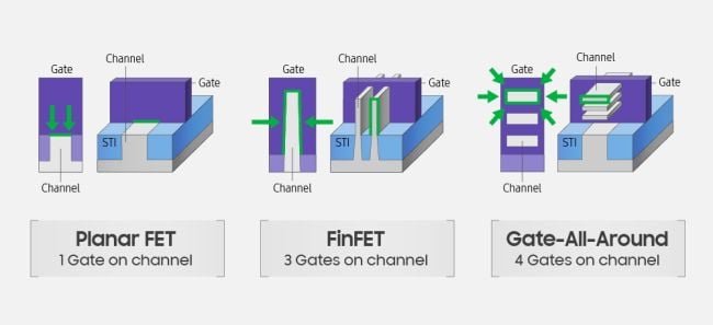
Interestingly, TSMC will be discarding the mostly-used FinFET process to adopt the new multi-bridge channel field effect transistor (MBCFET) architecture based on the surround gate (GAA) process. This helps to solve the physical limit of the FinFET’s current control leakage due to process shrinkage, helping to stuff more transistors in a small area.

The GAA (Gate-all-around, around the gate) process adopted by TSMC is not their sole weapon as Samsung too will implement this process but on the 3nm process. The GAA technology introduced by Samsung is Multi-Bridge Channel FET (MBCFET), which is actually a multi-channel bridge fin with a plate-like structure.

TSMC on track with 2nm process, gate-all-around (GAAFET) transistors will be used for the first time

The GAA process also has different forms and the current four mainstream technologies are – nanowires, sheet-like structure multi-way bridging fins, hexagonal cross-section nanowires, and nanorings. Each has its own advanatages, while GAA can really help reduce power consumption while maintaining performance gains.

However, the cost of implementing GAA is also very high and the cost of the 28nm process used to cost $62.9 million, while the newer 5nm process surged to $476 million. Samsung even claims that the cost of its own 3nm process based GAA may exceed the $500 million mark.

Do check out:

https://technosports.co.in/2020/09/23/microsoft-xbox-storage-expansion-card-rumored-to-increase-the-overall-cost-of-the-consoles/
Tags: 2nm processGAAFETTSMC
Previous Post

Intel launches 11th gen processors to power IoT applications

Next Post

Glance Launched Its First Exclusive Cricketainment Series with Danish Sait on Roposo

Related Posts

Technology

Free Premium AI Models Available in India Right Now

November 10, 2025
Technology

HyperOS 3 Testing Begins on 12 Xiaomi Phones—Final Update

November 10, 2025
FAQ

The BEST Google Play Redeem Codes as of November 2025

November 10, 2025
Technology

Dyson HP2 & HP1 Air Purifiers Launch to Battle India’s Smog

November 10, 2025
Technology

LG UltraGear G8 37G800A-B: 4K Gaming at 165Hz for $799

November 10, 2025
FAQ

Midas buy Redeem Codes Free UC and Skins in 2025: Check Out All Details

November 10, 2025
Next Post
Glance Launched Its First Exclusive Cricketainment Series with Danish Sait on Roposo

Glance Launched Its First Exclusive Cricketainment Series with Danish Sait on Roposo

Leave a Reply Cancel reply

Your email address will not be published. Required fields are marked *

This site uses Akismet to reduce spam. Learn how your comment data is processed.

TechnoSports Media Group

© 2025 TechnoSports Media Group - The Ultimate News Destination

Email: admin@technosports.co.in

  • Terms of Use
  • Privacy Policy
  • About Us
  • Contact Us

Follow Us

No Result
View All Result
  • Home
  • Technology
  • Smartphones
  • Deal
  • Sports
  • Reviews
  • Gaming
  • Entertainment

© 2025 TechnoSports Media Group - The Ultimate News Destination