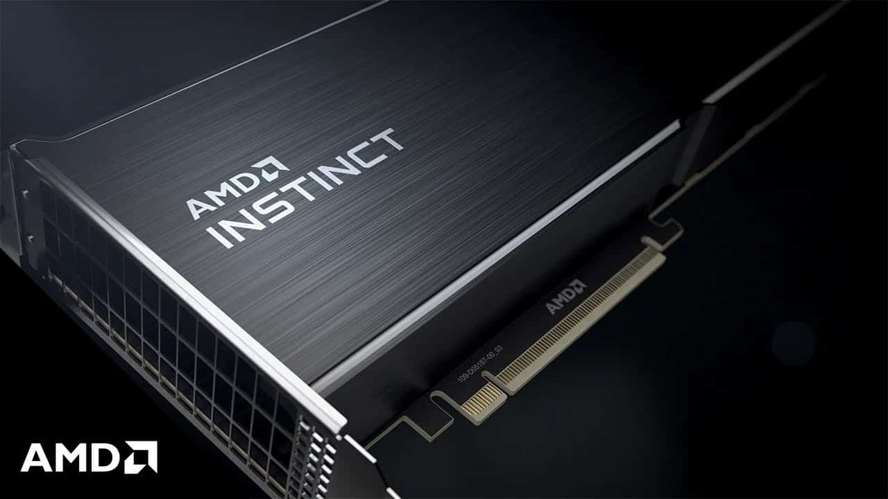
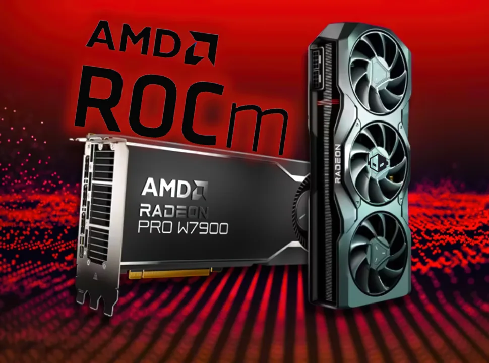
According to a recent leak, we now have a would-be confirmation of the configuration of the MI200 graphics processor. The latest leak comes from the ROCm software update which states that the accelerator offers 110 Compute Units.
However, something that isn’t yet made clear is whether this configuration refers to the whole card or just a single graphics chipset.
In the leaked news, the GPU ID string of GFX90A_110 suggests the configuration of the full MI200 accelerator or just one chipset, meaning that it is either the 220 CUs (2x 110) or 110 CUs (2x 55).
Many speculations are surrounding the MI200 accelerator, and according to the famous leaker @Kepler_L2, the MI300 will be featuring twice as many GPU dies as the MI200. All these rumours have one thing in common is that future AMD accelerators based on CDNA architectures will be going to continue to use the MCM design with an increasing number of GCD (Graphics Complex Die) or graphics tiles/chipsets.
There is likely not much information regarding the MI300 GPU and even its codename is not yet known, however, it is likely going to adopt a name after another giant star, such as Rigel or Antares.
| AMD Instinct Accelerators | ||||
| Accelerator Name | AMD Radeon Instinct MI60 | AMD Instinct MI100 | AMD Instinct MI200 | AMD Instinct MI300 |
| Architecture | 7nm GCN5 (GFX906) | 7nm CDNA1 (GFX908) | CDNA2 (GFX90A) | CDNA3 (?) |
| GPU | Vega 20 | Arcturus | Aldebaran (MCM) | ? (MCM) |
| Compute Tiles | 1 | 1 | 2 | 4 |
| Compute Units | 64 (64) | 120 | 2x 110 or 2x 55 | 4x (?) |
| FP32 Cores (Full GPU) | 4096 (4096) | 7680 (8192) | TBC | 4x (?) |
| GPU Clock Speed | 1800 MHz | ~1500 MHz | TBC | TBC |
| FP16 Compute | 29.5 TFLOPS | 185 TFLOPS | TBC | TBC |
| FP32 Compute | 14.7 TFLOPS | 23.1 TFLOPS | TBC | TBC |
| FP64 Compute | 7.4 TFLOPS | 11.5 TFLOPS | TBC | TBC |
| VRAM | 32 GB HBM2 | 32 GB HBM2 | 128 GB HBM2E | TBC |
| Memory Clock | 1000 MHz | 1200 MHz | TBC | TBC |
| Memory Bus | 4096-bit | 4096-bit | TBC | TBC |
| Memory Bandwidth | 1 TB/s | 1.23 TB/s | TBC | TBC |
| Form Factor | Dual Slot, Full Length | Dual Slot, Full Length | OAM | TBC |
| Cooling | Passive Cooling | Passive Cooling | TBC | TBC |
| TDP | 300W | 300W | TBC | TBC |


