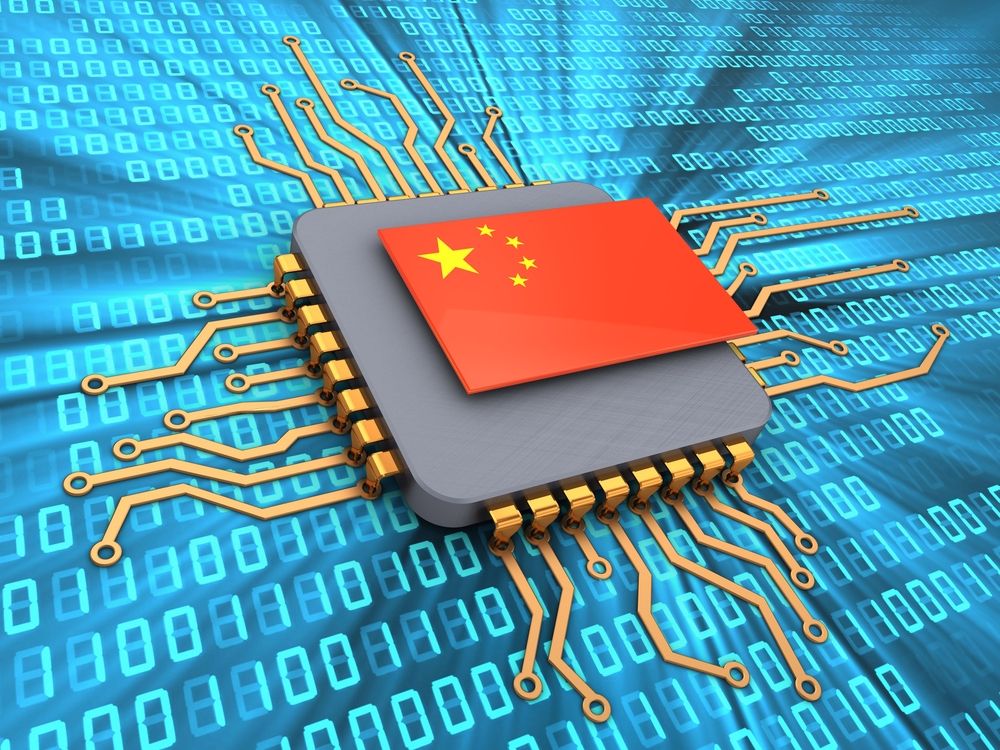
The Trade restrictions put on Chinese companies by the US administration have affected China’s semiconductor market the most. It’s house manufacturing plants have suffered tremendously due to their access to American technologies being cut off by the US administration. But the companies such as Huawei and SMIC soon learned to develop new technologies and innovations to become more self-dependent.
Recently the Shanghai-based Semiconductor Manufacturing International Corp (SMIC) stated that it had started small-scale trial production of its second-generation N+1 FinFET process. The announcement came at a time when its investors were questioning the company’s progress in the R&D and production of 7-nanometer products.
According to sources, SMIC first achieved mass production of the most advanced 14nm process in China in 2019. It is the company’s first-generation FinFET process, and it had deployed the process to manufacture the Hisilicon Kirin 710A chipset, which was utilized first on the Honor Play 4T and then a couple of other Huawei products.
This year, however, things were different as the company was facing various restrictions from the US administration, that its investors were getting anxious about the company’s progress. To this, the company responded that its second-generation FinFET N+1 process has indeed entered the customer introduction stage. It also hinted that it is expected to start small-scale production (trial production) by the end of 2020.
Earlier, INNOSILICON also announced that it had completed the world’s first chip tape-out and testing based on SMIC’s FinFET N+1 advanced process. All IPs are made in-house, with one-time functions. According to sources, the N+1 process is very similar to the 7nm process in terms of power and stability and does not require EUV lithography. Compared to the 14nm process, SMIC’s N+1 process can increase the performance by 20% and offers a 57% reduction in power consumption. And the company claims that the 7nm market benchmark performance also increases by 35%.