Quantum Dot Lasers: Revolutionary breakthrough makes photonic computing faster, smaller, and more affordable
Imagine shrinking a laser to fit inside your smartphone chip while making it 10 times more efficient. That’s exactly what researchers at UC have achieved with their groundbreaking quantum dot laser technology.
Table of Contents
The Game-Changing Discovery
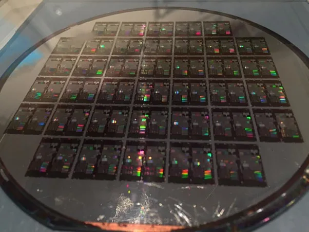
Dr. Rosalyn Koscica and her team have successfully integrated indium arsenide quantum dot lasers directly onto silicon photonics chiplets – something that seemed impossible just years ago. Published in the prestigious IEEE Journal of Lightwave Technology, this research solves a major manufacturing headache that has plagued the industry.
“Photonic integrated circuit applications call for on-chip light sources with a small device footprint to permit denser component integration,” explains Dr. Koscica.
Why This Matters for Tech
Traditional laser integration on silicon was like trying to build a house with incompatible materials. The structural mismatch between III-V semiconductors and silicon made manufacturing extremely challenging and expensive.
Key Technical Achievements
| Specification | Achievement |
|---|---|
| Operating Temperature | Up to 105°C |
| Lifespan | 6.2 years at 35°C |
| Wavelength | O-band (low dispersion) |
| Integration Method | Monolithic on-chip |
| Manufacturing | Scalable and cost-effective |
The Secret Recipe
The breakthrough combines three innovative approaches:
- Pocket laser strategy for seamless integration
- Two-step material growth using advanced deposition techniques
- Polymer gap-fill technology to minimize light loss
Real-World Impact
This technology opens doors for:
- Faster data centers with integrated photonic processors
- Smaller optical devices in consumer electronics
- Cost-effective manufacturing of photonic chips
- Enhanced 5G and 6G networks with better signal processing
For tech enthusiasts following the latest in semiconductor innovations and photonic computing advances, this represents a major leap toward practical quantum-enhanced devices.
What’s Next?
The scalable nature of this integration technique means we could see commercial applications within the next few years. As the demand for faster, more efficient computing grows, this quantum dot laser technology positions silicon photonics as the backbone of next-generation tech infrastructure.
Stay updated with the latest breakthroughs in quantum technology and chip manufacturing on TechnoSports.