At GTC 2022, Nvidia unveiled its Hopper architecture, revealing the H100 server accelerator but only displaying renders of it. The SXM edition of the card, which has a mind-boggling 700W TDP, has now been photographed in hand.
We’ve only seen renders of Nvidia’s H100 server accelerator, which is based on the Hopper architecture, for a little over a month now. Now, however, ServeTheHome has released images of the card in its SXM5 form factor.
The GH100 computing GPU has an 814 mm2 die size and is manufactured on TSMC’s N4 manufacturing node. The SXM model has 16896 FP32 CUDA cores, 528 Tensor cores, and 80GB of HBM3 memory, all coupled by a 5120-bit bus. There are six 16GB memory stacks around the GPU, as seen in the photos, but one of them is disabled.
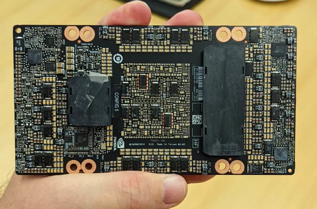
Below you can see the H100 GPU’s latest images
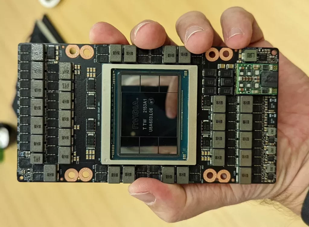
Nvidia also stated that the card’s TDP is 700W, which is 75% greater than its predecessor, so it’s no surprise that it has a powerful VRM solution. It has 29 inductors with two power stages apiece, as well as three inductors with only one power stage. Cooling all of these densely packed components will almost certainly be difficult.
The connector configuration for SXM5 is another significant modification. There is now a short and a long mezzanine connector, as opposed to two identically sized longer ones in earlier generations.
In the third quarter of this year, Nvidia will begin releasing H100-equipped devices. Although it has fewer CUDA cores, inferior HBM2e memory, and half the TDP of the SXM type, the PCIe version of the H100 is now advertised in Japan for 4,745,950 yen ($36,300) including taxes and shipping.
Also Read:
Apple’s Thunderbolt 4 Pro cable is the longest one yet in the market selling for a hefty ₹15900