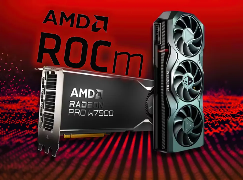
It’s not very far that new flagship GPUs from NVIDIA and AMD will make their way into the world soon enough, however, rumours surrounding their performance start to grow more than ever. Now there are interesting rumours from both Kopite7kimi and Greymon55 regarding both GPU series from the two giants and it is to be noted that both of them are quite accurate always.
As recently confirmed by Kopite7kimi the flagship GPU here, referred to as **90 could be called RTX 4090 which will use the upcoming AD102 flagship GPU and it is being said that the speed of the VRAM or GPU memory could be 21Gbps and not 24Gbps.
So, essentially, even the next-gen Ada Lovelace flagship GPU will be using the same memory as we see on the recently launched RTX 3090 Ti. However, it will use a huge 24GB VRAM and suck 600W of power, even the board numbers that have been accurately leaked by Kopite7kimi, which could be verified as we get closer to the launch.
Now coming to AMD’s rumours brought to you by Greymon55, the Red team too is very serious with RDNA3 and potential rumours suggesting AMD could surpass or equal NVIDIA’s top-of-the-line flagship GPUs. AMD is confirmed to use a multi-chip design for the first time on its GPUs using an interconnect that connects the MCD chiplets.
So, the tipster has suggested the flagship Navi 31 GPU will use 7 chiplets, out of the 2 will be manufactured using 5nm TSMC process and four of them by 6nm process and there will be one interconnected controller to connect the dies.
via Videocardz


