In order to explore collaboration with regional partners, Lisa Su, AMD’s CEO, and other corporate C-level executives want to travel to Taiwan in late September or early November. The management of AMD plans to meet with major PC manufacturers, chip packaging experts, and Taiwan Semiconductor Manufacturing Co.
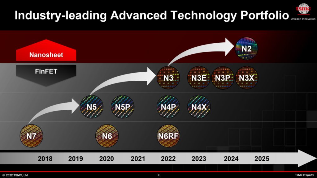
During her visit, Lisa Su intends to talk about potential future collaboration with TSMC’s CEO, CC Wei. The use of TSMC’s “N3 Plus” fabrication node (likely N3P) and N2 (2nm-class) production technology is one of the subjects, according to sources with knowledge of the situation, according to DigiTimes. The chief executives of the two companies will also talk about plans for new orders, including technology that are either already accessible or will be in the near future.
The excellent success that AMD has experienced recently is largely due to TSMC’s capacity to manufacture chips in large quantities utilising its fiercely competitive process technology
AMD must assure adequate allocation at TSMC and early access to the foundry’s most recent process design kits if it is to continue its streak of roaring success (PDK). It is about time for AMD to start discussing the use of N2 for its 2026 products and beyond since TSMC will begin volume chip production on its N2 node sometime in the second half of 2025.
Future success of AMD will be dependent on modern chip packing technologies as well as advanced TSMC semiconductor manufacturing technologies since the company (like other chip designers) will heavily rely on multi-chiplet chip packaging technologies.
Therefore, Lisa Su from AMD will also talk about their partnership with TSMC, Ase Technology, and SPIL for innovative packaging. According to DigiTimes, AMD now employs TSMC’s 3D SoIC (system on integrated chips) platform, including CoWoS (chip on wafer on substrate) packaging technology and Ase’s fan-out embedded bridge (FO-EB) packaging technique, for certain of its products. However, when novel packaging becomes more widely used over time, AMD will need to negotiate pricing and allocation well in advance.
Along with discussing longer-term plans, AMD’s C-level executives will also talk about more practical issues, such as how to get the advanced printed circuit boards (PCBs) needed for its CPUs, which is one of the things limiting AMD server CPU shipments, as well as how to get Ajinomoto build-up films (ABF) for these PCBs from partners like Unimicron Technology, Nan Ya PCB, and Kinsus Interconnect Technology.
The executives of AMD will also meet with ASMedia, which creates chipsets for the red firm, and Asus and Acer, two sizable Taiwanese PC manufacturers with strong ties to the American chip designers.
Also Read: