Intel unveiled a slew of new announcements at IEDM 2021 that will help to propel and accelerate Moore’s Law beyond 2025. These innovations include quantum physics breakthroughs, new packaging, and transistor technologies, and much more.
Intel is revealing key packaging, transistor, and quantum physics breakthroughs critical to advancing and accelerating computing well into the next decade as part of its relentless pursuit of Moore’s Law. Intel outlined its path to more than 10x interconnect density improvement in packaging with hybrid bonding, 30 percent to 50 percent area improvement in transistor scaling, breakthroughs in new power and memory technologies, and new physics concepts that could one day revolutionize computing at the IEEE International Electron Devices Meeting (IEDM) 2021.
“At Intel, the research and innovation necessary for advancing Moore’s Law never stop. Our Components Research Group is sharing key research breakthroughs at IEDM 2021 in bringing revolutionary process and packaging technologies to meet the insatiable demand for powerful computing that our industry and society depend on. This is the result of our best scientists’ and engineers’ tireless work. They continue to be at the forefront of innovations for continuing Moore’s Law.”
–Robert Chau, Intel Senior Fellow, and general manager of Components Research
Moore’s Law has been tracking computing breakthroughs from mainframes to mobile phones to fulfill the demands of each technology generation. Today, as we enter a new era of computing, with boundless data and artificial intelligence, this process is ongoing.
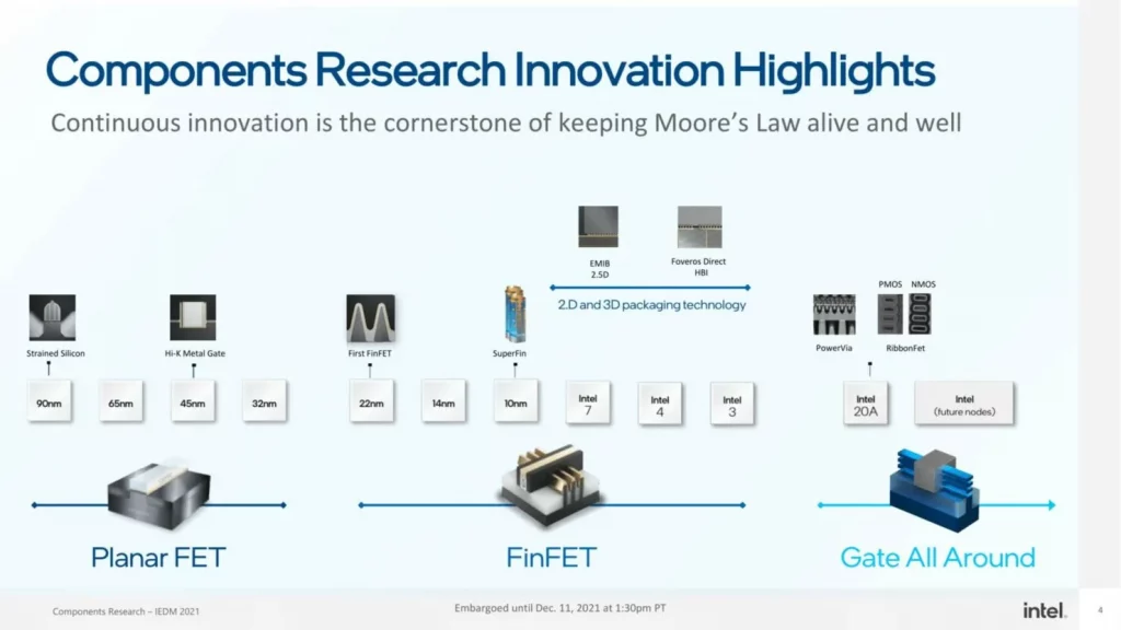
Moore’s Law is based on the principle of continuous innovation. Intel’s Components Research Group is focused on three areas of innovation: crucial scaling technologies for delivering more transistors, novel silicon capabilities for power and memory improvements, and physics investigation to transform the way the world computes. Component Research was responsible for many of the inventions that broke past prior Moore’s Law boundaries and are now found in today’s devices, including strained silicon, Hi-K metal gates, FinFET transistors, RibbonFET, and packaging advancements including EMIB and Foveros Direct.
Through its three areas of pathfinding, Intel is on track to continue the advancement and benefits of Moore’s Law well beyond 2025, as evidenced by the breakthroughs revealed at IEDM 2021.
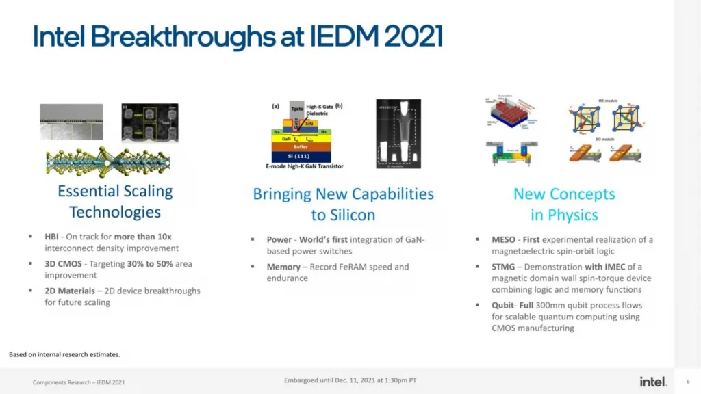
Intel is investing heavily in key scaling technologies to deliver more transistors in future product offerings:
The company’s researchers have proposed solutions for the design, process, and assembly challenges of hybrid bonding interconnect, predicting a 10x increase in interconnect density in packaging. Intel announced plans to introduce Foveros Direct, which will enable sub-10-micron bump pitches and an order of magnitude increase in interconnect density for 3D stacking, at the Intel Accelerated event in July. Intel is also calling for the creation of new industry standards and testing procedures to enable a hybrid bonding chipset ecosystem so that the ecosystem can benefit from advanced packaging.
Beyond its gate-all-around RibbonFET, Intel is preparing for the post-FinFET era by stacking multiple (CMOS) transistors to provide a maximum 30 percent to 50 percent logic scaling gain for Moore’s Law’s continuous growth by fitting more transistors per square millimeter.
Intel is also paving the way for Moore’s Law to advance into the angstrom era with forward-looking research that shows how novel materials as thin as a few atoms can be used to make transistors that overcome the limitations of conventional silicon channels, allowing millions more transistors per die area for ever-more-powerful computing in the next decade.
Intel is giving silicon new capabilities
The world’s first integration of GaN-based power switches with silicon-based CMOS on a 300 mm wafer is advancing more efficient power technologies. This paves the way for low-loss, high-speed power delivery to CPUs while also reducing motherboard components and space requirements.
Intel’s industry-leading low-latency read/write capabilities using novel ferroelectric materials for possible next-generation embedded DRAM technology that can deliver more memory resources to address the growing complexity of computing applications, from gaming to AI, are another advancement.
With silicon transistor-based quantum computing, Intel is targeting huge performance, as well as wholly new switches for tremendously energy-efficient computation with revolutionary room-temperature devices. These breakthroughs could eventually replace traditional MOSFET transistors by employing whole new physics concepts:
Intel exhibited the world’s first experimental realization of a magnetoelectric spin-orbit (MESO) logic circuit at ambient temperature at IEDM 2021, demonstrating the potential for a new type of transistor based on switching nanoscale magnets to be manufactured.
Intel and IMEC are working on spintronic materials research to bring device integration research closer to a fully functional spin-torque device.
Intel also demonstrated full 300 mm qubit process flows for scalable quantum computing that is compatible with CMOS production, as well as the next stages for further research.
also read:
Intel CEO rumoured to visit TSMC to bid for its advanced chip manufacturing process