Intel will soon be launching its first generation Arc graphics and recently we have witnessed the leak of the upcoming graphics cards nomenclature. Intel has created a usage guide for add-in board members and this includes the details that we had not seen before which also contains the fact that the generations will be referred to as Intel Arc XXXX, XXXX, cXXX, and XXXX respectively.
According to the leaked design document, the first generation of GPUs will be referred to as Intel Arc a-series as well as Intel Arc a-series graphics however they will not be referred to as 1st generation Intel Arc graphics.
Here are some of the most likely guesses circling the internet:
- Intel Arc a300, a500 and a700 (performance-wise)
- Intel Arc a130, a150 and a170 (performance-wise)
- Intel Arc a800, a600, and a200 (referring to the number of Xe slices)
let’s come to the first variant of the Intel Xe HPG GPU as it’s expected to have 8 slices, each consisting of 4 Xe Cores. This will make for a total Vector/Matrix count of 512 (8x4x16).
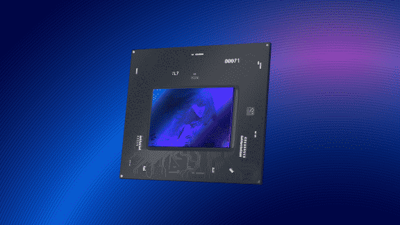
In the world of graphics, there is an insatiable demand for better performance and more realism. TSMC is excited that Intel has chosen our N6 technology for their Alchemist family of discrete graphics solutions.
There are many ingredients to a successful graphics product including semiconductor technology. With N6, TSMC provides an optimal balance of performance, density, and power efficiency that are ideal for modern GPUs. We are pleased with the collaboration with Intel on the Alchemist family of discrete GPUs.
Dr. Kevin Zhang,
Senior Vice President of Business Development at TSMC
Coming to the information which we already have about the Intel Xe HPG, the card will be manufactured on TSMC’s 6nm process, which should give them quite the kick in terms of power efficiency and transistor density. Intel’s Xe HPG architecture is expected to be capable of achieving 1.5x higher clock rates than Xe LP can also deliver 1.5x higher performance per watt.