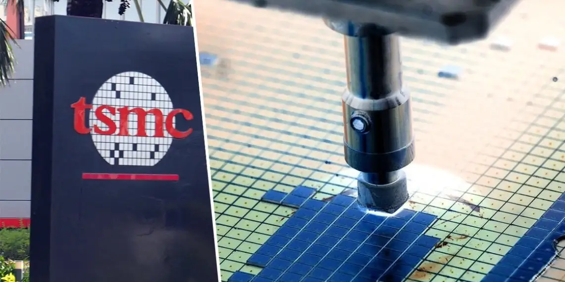
Although TSMC’s N3 (3nm-class) family of fabrication processes offers a number of advantages in terms of performance and power, the foundry’s initial N3 node is prohibitively expensive, preventing widespread adoption. Unsurprisingly, according to MyDrivers, the company is preparing to lower its quotes for 3nm production in order to pique the interest of chip designers.
While any published TSMC N3 quotes and prices should be regarded as rumours at this time, it is likely that TSMC’s production costs on its N3E process will be lower than those on its initial N3. It’s unclear how much the company will charge for production on other N3-class nodes like the N3P, N3S, and N3X. Lowering the cost of 3nm production will attract more customers to these nodes, but this will not happen overnight.
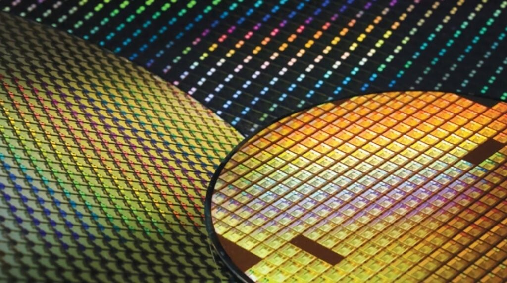
Apple is rumoured to be the sole user of TSMC’s initial N3 manufacturing technology (also known as N3B) because the company is the foundry’s largest client willing to adopt cutting-edge nodes ahead of others. However, using N3 is an expensive technology. According to China Renaissance, N3 extensively uses extreme ultraviolet (EUV) lithography for up to 25 layers, and each EUV scanner now costs $150 million to $200 million, depending on configuration.
To compensate for the depreciation of fabs equipped with such production tools, TSMC must charge a higher price for production on its N3 process and successors.
It is also believed that TSMC may charge up to $20,000 per N3 wafer, and while such quotes are subject to a variety of factors, the main takeaway is that chip production is becoming increasingly expensive. Increased costs mean lower profits for companies like AMD, Broadcom, MediaTek, Nvidia, and Qualcomm, so chip designers are rethinking how they create advanced designs and use cutting-edge nodes.
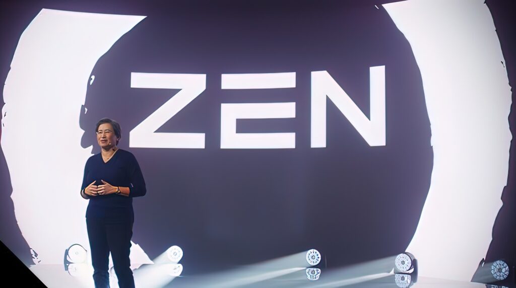
“We believe the meaningful [N3] ramp-up will be in 2H 2023 when the optimized version, N3E, will be ready,” wrote Szeho Ng, an analyst with China Renaissance. “Its major customers in HPC (i.e., AMD, Intel), smartphone (i.e., QCOM, MTK) and ASIC (i.e., MRVL, AVGO, GUC) will likely stay in N4/5 and choose N3E as their maiden N3 class foray, in our view. Meanwhile, we believe the baseline N3 (aka N3B) adoption will be largely limited to Apple products.”
TSMC is reportedly considering lowering its quotes for these nodes in order to encourage its partners to use its N3-class process technologies. TSMC’s N3E process, in particular, uses EUV only for up to 19 layers, has a lower manufacturing complexity, and is thus less expensive to use. TSMC could reduce N3E production quotes without jeopardising profitability. When it comes to SRAM cell scaling, N3E has no advantages over N5, resulting in larger die sizes when compared to those made on N3/N3B.
AMD publicly announced plans to use a N3 node for some of its Zen 5-based designs due in 2024, while Nvidia is expected to use N3 for its next-generation Blackwell architecture-based GPUs due around the same time. Adoption of N3-class nodes is expected to be limited to specific products due to high costs.
Also Read: