This year along with the Instinct MI200 accelerator, AMD is also planning to release its CDNA 2 powered Aldebaran GPU. The graphics processor will feature an MCM design and carry massive amounts of cores and memory. In the latest leak, we can also witness a die block diagram of the full Aldebaran GPU.
According to sources, the block diagram shows the latest details shared by Kepler_L2 for the CDNA 2 powered GPU. The Aldebaran GPU powering the Instinct MI200 will feature two dies, a secondary and a primary. The two dies will each consist of 8 shader engines for a total of 16 SE’s.
It’s not just that, but the block diagram suggests that each of the Shader Engine will pack 16 CUs with full-rate FP64, packed FP32 & a 2nd Generation Matrix Engine for FP16 & BF16 operations.
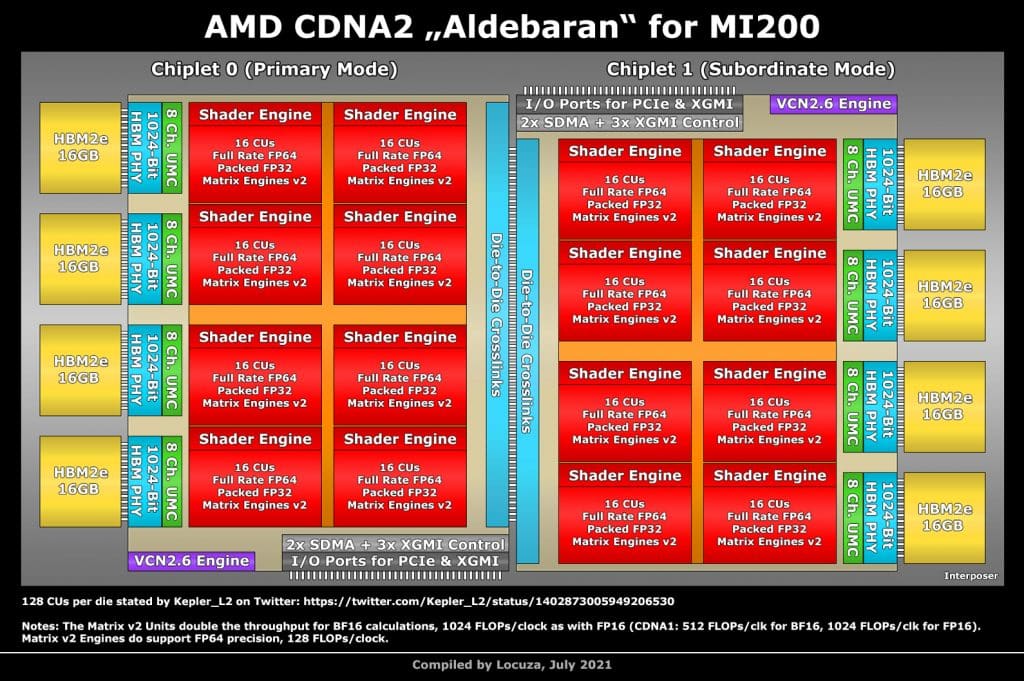
Each die of the block diagram will comprise 128 compute units or 8192 stream processors. So we can assume that a total of 256 compute units or 16,384 stream processors for the entire chip will be present, as well as the Aldebaran GPU will be powered by a new XGMI interconnect.
Moving over to DRAM, AMD has gone with an 8-channel interface consisting of 1024-bit interfaces for an 8192-bit wide bus interface. Each interface can support 2GB HBM2e DRAM modules. This should give us up to 16 GB of HBM2e memory capacity per stack, and since there are eight stacks in total, the total capacity would be a whopping 128 GB. That’s 48 GB more than the A100, which houses 80 GB HBM2e memory. This would be a juggernaut of an HPC GPU, but we also expect some high power figures when it launches.
As for the product itself, Kepler_L2 states that the actual AMD Instinct MI200 accelerator will utilize a cut-down configuration comprising 224 CUs or 14,336 cores.
AMD Radeon Instinct Accelerators 2020
| Accelerator Name | AMD Radeon Instinct MI6 | AMD Radeon Instinct MI8 | AMD Radeon Instinct MI25 | AMD Radeon Instinct MI50 | AMD Radeon Instinct MI60 | AMD Instinct MI100 | AMD Instinct MI200 |
| GPU Architecture | Polaris 10 | Fiji XT | Vega 10 | Vega 20 | Vega 20 | Arcturus (CDNA 1) | Aldebaran (CDNA 2) |
| GPU Process Node | 14nm FinFET | 28nm | 14nm FinFET | 7nm FinFET | 7nm FinFET | 7nm FinFET | Advanced Process Node |
| GPU Cores | 2304 | 4096 | 4096 | 3840 | 4096 | 7680 | 14,336? |
| GPU Clock Speed | 1237 MHz | 1000 MHz | 1500 MHz | 1725 MHz | 1800 MHz | ~1500 MHz | TBA |
| FP16 Compute | 5.7 TFLOPs | 8.2 TFLOPs | 24.6 TFLOPs | 26.5 TFLOPs | 29.5 TFLOPs | 185 TFLOPs | TBA |
| FP32 Compute | 5.7 TFLOPs | 8.2 TFLOPs | 12.3 TFLOPs | 13.3 TFLOPs | 14.7 TFLOPs | 23.1 TFLOPs | TBA |
| FP64 Compute | 384 GFLOPs | 512 GFLOPs | 768 GFLOPs | 6.6 TFLOPs | 7.4 TFLOPs | 11.5 TFLOPs | TBA |
| VRAM | 16 GB GDDR5 | 4 GB HBM1 | 16 GB HBM2 | 16 GB HBM2 | 32 GB HBM2 | 32 GB HBM2 | 64/128 GB HBM2e? |
| Memory Clock | 1750 MHz | 500 MHz | 945 MHz | 1000 MHz | 1000 MHz | 1200 MHz | TBA |
| Memory Bus | 256-bit bus | 4096-bit bus | 2048-bit bus | 4096-bit bus | 4096-bit bus | 4096-bit bus | 8192-bit |
| Memory Bandwidth | 224 GB/s | 512 GB/s | 484 GB/s | 1 TB/s | 1 TB/s | 1.23 TB/s | ~2 TB/s? |
| Form Factor | Single Slot, Full Length | Dual Slot, Half Length | Dual Slot, Full Length | Dual Slot, Full Length | Dual Slot, Full Length | Dual Slot, Full Length | Dual Slot, Full Length / OAM |
| Cooling | Passive Cooling | Passive Cooling | Passive Cooling | Passive Cooling | Passive Cooling | Passive Cooling | Passive Cooling |
| TDP | 150W | 175W | 300W | 300W | 300W | 300W | TBA |