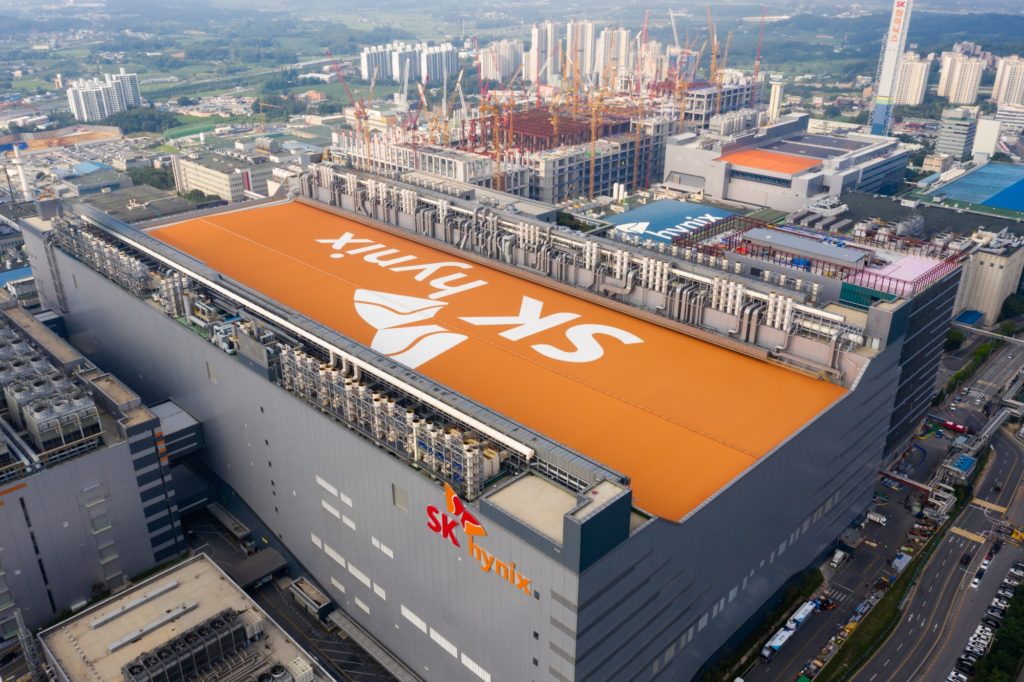
South Korea’s SK Hynix plans to choose a U.S. location for its advanced chip packaging plant and start construction there around the first quarter of next year. This will help the United States compete as China pours money into the expanding sector.
The mill would ramp up to mass production by 2025–2026 and employ roughly 1,000 people, according to one of the individuals, who declined to be named since information about the plant has not been made public. The plant’s estimated cost would be “many billions.”
One of the people stated that the corporation “hopes to make a selection of the site and break ground somewhere around the first quarter of next year.”
The new plant was unveiled last month as a part of a $22 billion U.S.-based investment package in semiconductors, green energy, and bioscience projects by SK Group, South Korea’s second-largest conglomerate and owner of memory chipmaker SK Hynix (000660. KS).
The White House announced that the semiconductor sector would get $15 billion in funding for research and development initiatives, materials, and the construction of a cutting-edge packaging and testing facility.
SK Hynix acknowledged that it will choose a location for the facility in the first half of 2023, but it insisted that no choice had been made regarding the timing of construction.
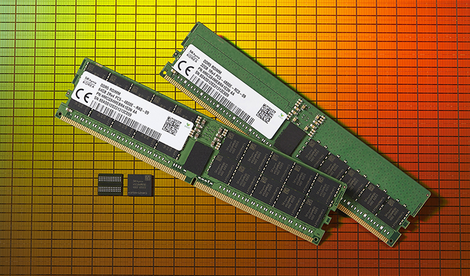
The majority of low-value, basic chip packaging processes were long ago transferred from the United States to foreign companies, primarily in Asia. At these factories, chips are put into protective frames and tested before being sent to electronics makers.
However, new frontlines are being formed in the competition to create innovative packaging methods, which combine many chips with various functionalities into a single package to improve overall capabilities and contain the cost of more sophisticated processors.
According to the report, a senior executive at China’s largest chipmaker SMIC (0981. HK), which was placed on a U.S. trade blacklist in 2020, suggested last year that Chinese businesses should concentrate on innovative packaging to make up for their inadequacies in producing more complex chips.
The CHIPS Act, which provides $52 billion in subsidies for chip production and research as well as an anticipated $24 billion in investment tax credits for chip factories, was signed into law this week by Vice President Biden, prompting SK Group’s action. According to the sources, both the chip packaging plant and the R&D facilities would be eligible for the funds.
In recent years, American chipmakers have announced a flurry of expansion ambitions, including Taiwan Semiconductor Manufacturing Co (2330. TW), Samsung Electronics (005930. KS), and Intel (INTC.O).
Also read: