SK Hynix is set to embark on an endeavour by investing $1 billion to upgrade its existing semiconductor packaging facilities. This strategic move comes at a time of increasing demand, for artificial intelligence (AI) technologies, which has surged to new levels.
Notably, industry giants such as NVIDIA and AMD have shown interest in SK Hynix, considering the Korean company as their preferred source for High Bandwidth Memory (HBM). The proof of this can be seen in SK Hynix experiencing a depletion of this year’s supply indicating the rising demand for its products.

More About SK Hynix Expanding Semiconductor Facilities
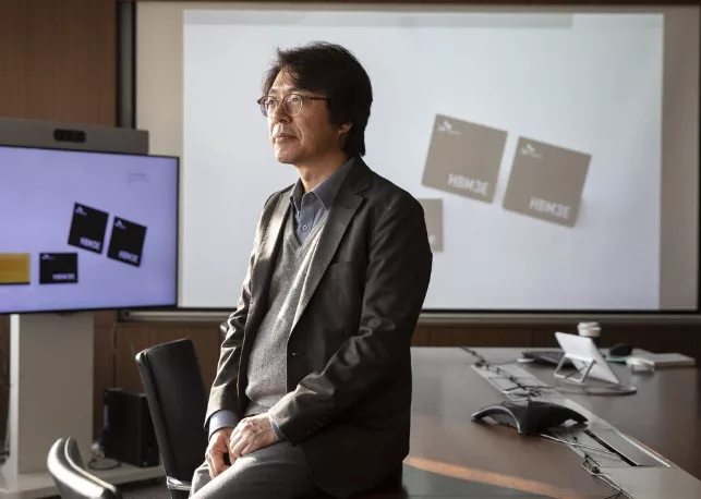
In preparation for a year in 2025, the company is taking proactive steps to address the industry’s high demand. According to reports from BNN Bloomberg and shared by the company’s Head of Packaging Development Lee Kang Wook, SK Hynix is investing $1 billion to expand its facilities in South Korea.
This significant investment underscores the company’s dedication to improving chip packaging, recognized as the frontier in semiconductor markets. With HBM playing a role in powering AI devices and advancing computing capabilities progress packaging is considered vital.
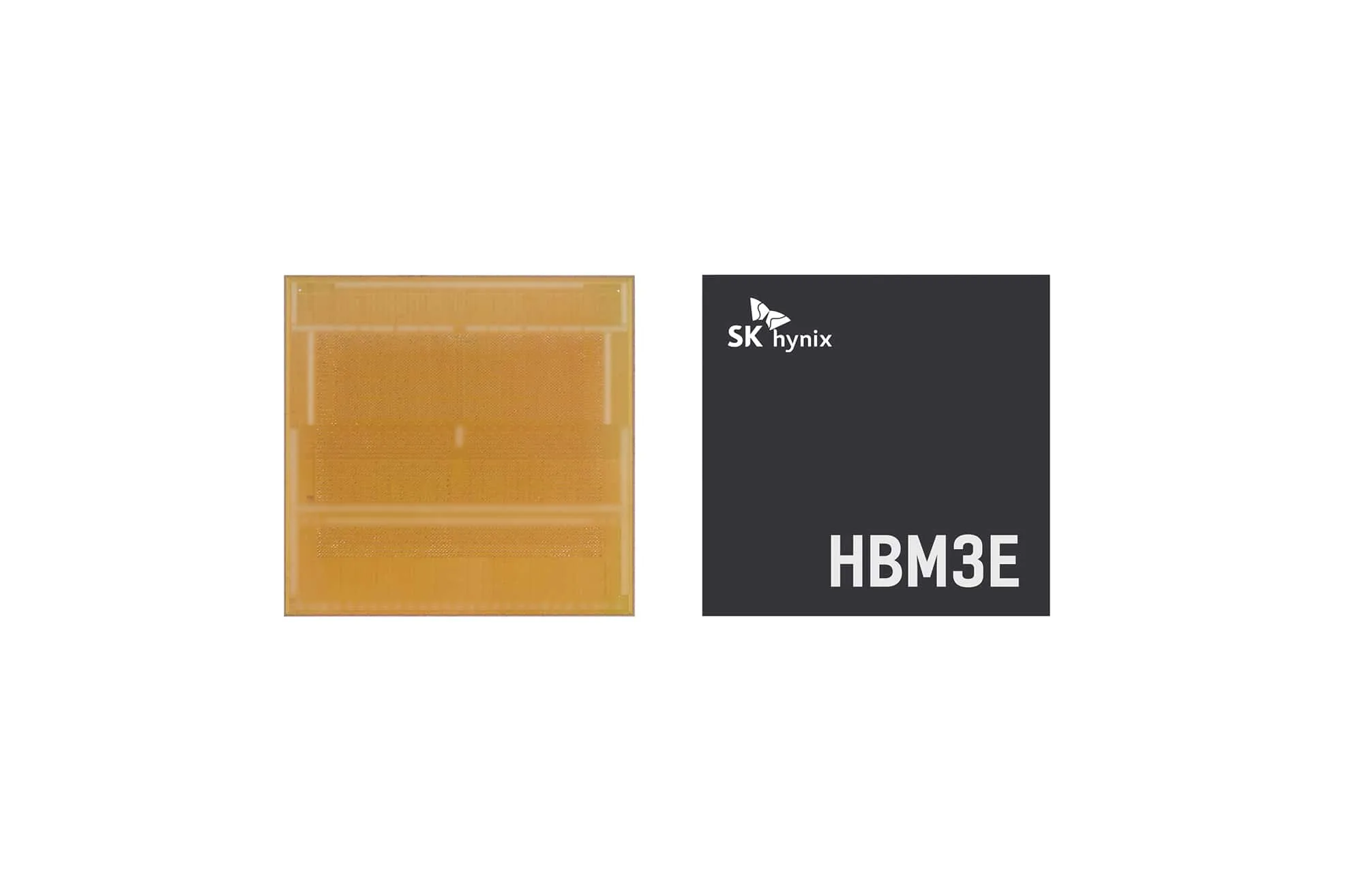
Looking forward, the company is gearing up for an era of innovation. The Korean manufacturer is fully committed to the industry and is ready to advance its progress, in the HBM sector. Recent updates suggest that the company has moved forward to test its 12-layer HBM3E variant, with samples sent for qualification tests to NVIDIA. Moreover, talks are circulating about SK Hynix’s partnership with TSMC to jointly work on HBM standards like HBM4 for future AI GPUs.
The HBM industry landscape is increasingly competitive, with players like SK Hynix, Micron, Samsung Foundry, and others striving to introduce their solutions to the market. The key differentiator lies in how each company addresses the overwhelming demand while embracing an innovative approach to meet the evolving needs of the industry.