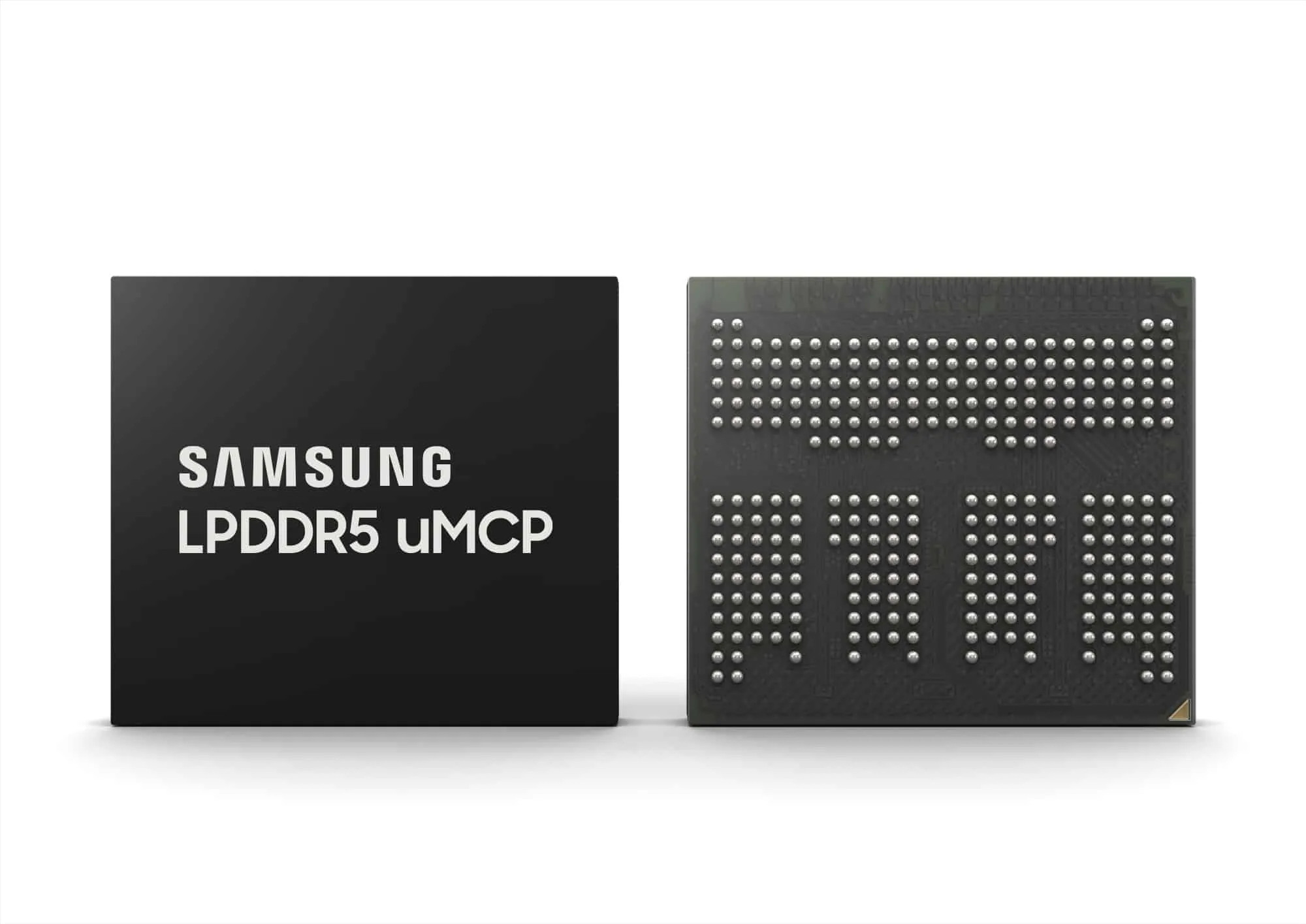
Samsung Electronics, yesterday made a huge announcement stating that it has already begun the mass production of its latest smartphone memory solution, the LPDDR5 UFS-based multichip package (MCP). Being a global leader in-memory technology, the South Korean-based tech giant has longed before announced its plans of incorporating its fastest LPDDR5 DRAM with the latest UFS 3.1 NAND flash. The company stated that this allows the company to deliver flagship-level performance to a much broader range of smartphone users.
“Samsung’s new LPDDR5 uMCP is built upon our rich legacy of memory advancements and packaging know-how, enabling consumers to enjoy uninterrupted streaming, gaming, and mixed reality experiences even in lower-tier devices. As 5G-compatible devices become more mainstream, we anticipate that our latest multichip package innovation will accelerate the market transition to 5G and beyond, and help to bring the metaverse into our everyday lives a lot faster.”
When compared to the latest mobile DRAM and NAND interfaces, Samsung’s MCP can deliver lightning-fast speed and high storage capacity at very low power. This is a much-needed combination now that the implementation of 5G in smartphones is increasing every day and numerous 5G applications such as advanced photography, graphics-intensive gaming, and augmented reality (AR) can be made possible on a non-flagship chip.
According to official sources, just by integrating DRAM and NAND storage into a single compact package that measures only 11.5mm x 13mm, the new chip will maximize space efficiency within a smartphone. The capacity of DRAM can be expanded from 6 gigabytes (GB) to 12GB and storage options from 128GB to 512GB.
The South Korean company also announced that it has completed compatibility testing of the LPDDR5 MCP. The company also announced that its MCP-equipped devices to hit mainstream markets starting this month.