As the business wants to expand its supply chain, Samsung is reportedly aiming to supply HBM3 memory and packaging facilities to NVIDIA for its AI GPUs. TSMC now dominates NVIDIA’s orders for wafer fabrication and sophisticated 2.5D semiconductor packaging.
However, it has been stated that TSMC is unable to satisfy NVIDIA’s demand due to a big surge of orders, which is why the business is now intending to employ a dual-sourcing approach to assure a consistent supply chain.
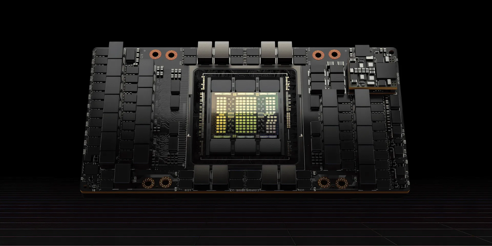
SK Hynix now supplies the major memory chips used in the AI GPU, HBM3. TSMC has highlighted worries about the massive workload associated with these chips’ 2.5D CoWoS packaging. This has prompted NVIDIA to seek alternative suppliers, including Amkor Technology of the United States and Siliconware Precision Industries Taiwan (SPIL), as previously reported by DigiTimes. Samsung has also entered the market through its AVP (Advanced Package) division, providing NVIDIA with a unique offering.

According to reports, Samsung proposed to buy TSMC semiconductor wafers and HBM3 memory from its memory division. Using the company’s unique I-Cube 2.5D packaging, Samsung has arranged for NVIDIA to potentially have a supplier accountable for all development stages. Furthermore, the corporation has vowed to recruit additional engineers to this work, with the possibility of directly procuring the semiconductor wafer from the foundry division in the future.
Samsung has already begun mass production of HBM3 memory, with sources claiming that the memory has quicker speeds (6.4 GB/s) and lower energy consumption than SK Hynix.
The technique has gained popularity, particularly among AMD’s newer MI300 Instinct APUs, which include Samsung’s HBM3. If the NVIDIA transaction goes through, the company might gain 10% of the entire order volume.
The quality of the south korean company’s HBM3 and 2.5D packaging, as well as whether it meets NVIDIA’s specifications, will be the decisive factors in this agreement. Technically, Samsung and TSMC are competing, with both companies rapidly constructing facilities to serve their partners. If Samsung earns NVIDIA’s trust through its products, TSMC will be in jeopardy, and its market share may be at threat.
However, rest confident that this transaction is complicated, and it may damage the NVIDIA-TSMC partnership, which will not benefit either company. However, one thing is certain: the south korean tech giant is pressing the accelerator in this space, whether through its foundry or memory division. It would be interesting to see how things play out, especially in light of a recent report indicating that Samsung is ahead of TSMC in terms of yield rates and fabrication technologies.
Also Read: