Rambus Incorporated, founded in 1990, is an American technology company that designs, develops and licenses chip interface technologies and architectures that are used in digital electronics products. The company is well known for inventing RDRAM and for its intellectual property-based litigation following the introduction of DDR-SDRAM memory.
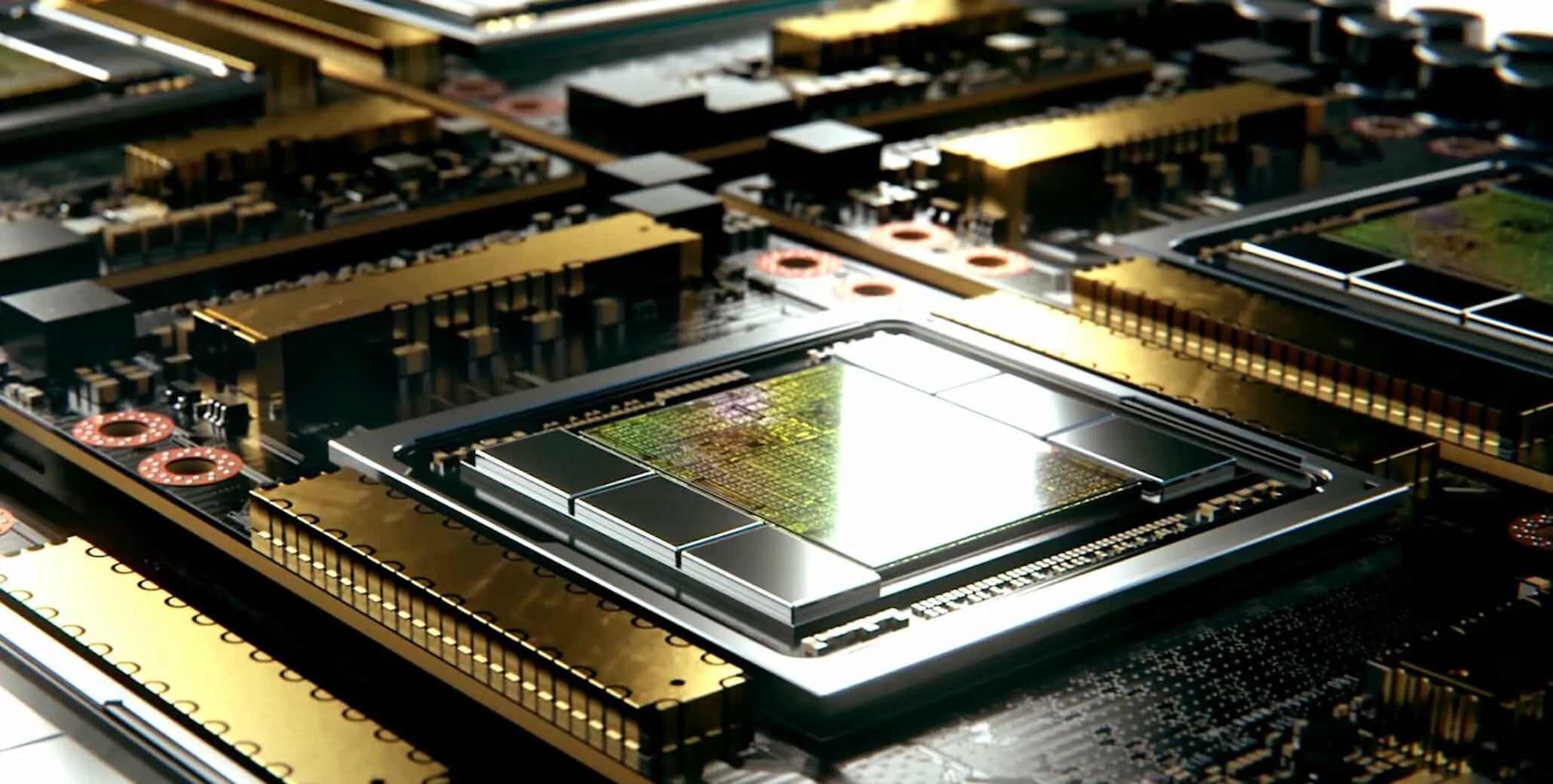
Rambus, a renowned chip manufacturer has just announced that it has completed the development of its advanced HBM3 memory subsystem. According to the manufacturer, this memory subsystem can hit transfer speeds of up to 8.4 Gbps.
Currently, in the market, we have the HBM2E which boasts to be the fastest memory option available and offer transfer rates of up to 3.2 Gbps. However, the HBM3 aims to offer more than double the speed of the current market standard offering an insane 8.4 Gbps transfer speed resulting in higher bandwidth.
According to sources, a single HBM2E package can peak out at 460 GB/s bandwidth however an HBM3 will offer up to 1.075 TB/s bandwidth which is 2x the total bandwidth jump.
Rambus had this to say about the technology:
The memory bandwidth requirements of AI/ML training are insatiable with leading-edge training models now surpassing billions of parameters,” said Soo Kyoum Kim, associate vice president, Memory Semiconductors at IDC. “The Rambus HBM3-ready memory subsystem raises the bar for performance enabling state-of-the-art AI/ML and HPC applications.”
Rambus achieves HBM3 operation of up to 8.4 Gbps leveraging over 30 years of high-speed signalling expertise, and a strong history of 2.5D memory system architecture design and enablement. In addition to the fully integrated HBM3-ready memory subsystem, Rambus provides its customers with interposer and package reference designs to speed their products to market.
“With the performance achieved by our HBM3-ready memory subsystem, designers can deliver the bandwidth needed by the most demanding designs,” said Matt Jones, general manager of Interface IP at Rambus. “Our fully-integrated PHY and digital controller solution builds on our broad installed base of HBM2 customer deployments and is backed by a full suite of support services to ensure first-time-right implementations for mission-critical AI/ML designs.”
Let’s look at some benefits of the Rambus HBM3-ready Memory Interface Subsystem:
- Supports up to 8.4 Gbps data rate delivering bandwidth of 1.075 Terabytes per second (TB/s)
- Reduces ASIC design complexity and speeds time to market with fully integrated PHY and digital controller
- Delivers full bandwidth performance across all data traffic scenarios
- Supports HBM3 RAS features
- Includes built-in hardware-level performance activity monitor
- Provides access to Rambus system and SI/PI experts helping ASIC designers to ensure maximum signal and power integrity for devices and systems
- Includes 2.5D package and interposer reference design as part of IP license
- Features LabStation development environment that enables quick system bring-up, characterization, and debugs
- Enables the highest performance in applications including state-of-the-art AI/ML training and high-performance computing (HPC) systems
Many in the industry expect the first generation of HBM3 memory to be very similar to HBM2E, meaning that in terms of capacity it should be made up of 16Gb DRAM Dies for a total of 16 GB (8-hi stack).
However, there are reports that the memory densities of HBM3 will increase once the specifications are finalized by JEDEC. It also reported that products such as the AMD’s Instinct Accelerators based on next-gen CDNA architecture, NVIDIA’s Hopper GPUs, and Intel’s future HPC accelerators based on next-gen Xe-HPC architecture, all possess the HDM3 memory stack.