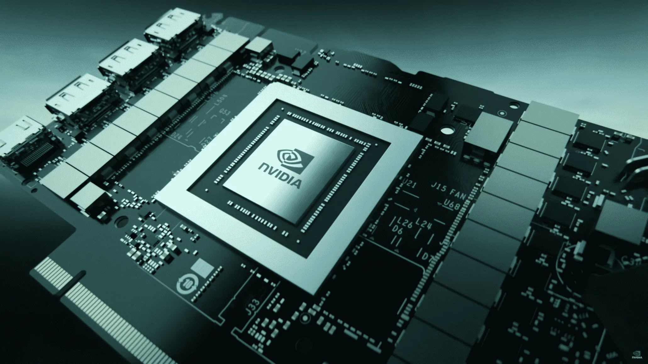
Earlier it was reported that a GPU called the Ampere GA102-250 GPU SKU exists In Nvidia’s sectors. Now a user on Hardwareluxx Forums has confirmed that the GPU which was previously expected to be featured on the GeForce RTX 3080 Ti graphics card exists.
According to sources, the GPU was spotted when the forum member took apart his GeForce RTX 3090, and the GPU was initially labeled as the GA102-250 SKU instead of the GA102-300 which is supposed to be the official SKU used on the RTX 3090.
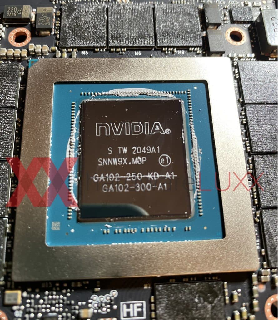
Until now, the NVIDIA GA102-250-KD-A1 GPU only existed in rumors, but now it is confirmed to be a real chip. The GPU was initially planned for the GeForce RTX 3080 Ti graphics card, but it seems that the green team decided to utilize it for the GeForce RTX 3090 graphics card.
The image posted by the user, clearly shows that the GA102-250-KD-A1 GPU label has been cut-off, and instead, it’s been repurposed as the GA102-300-A1 SKU. According to previous reports, we had heard that the GA102-250-KD-A1 was expected to feature 78 SM units enabled for a total of 9984 CUDA cores whereas the RTX 3090 with its GA102-300-A1 GPU packs 82 SMs or 10496 cores.
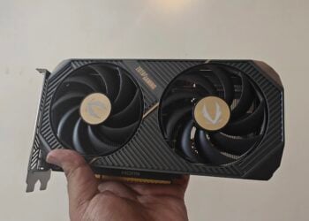
It is also being speculated that NVIDIA decided to repurpose the GA102-250 SKU into GA102-300 due to the shortages of its high-end graphics cards. The NVIDIA GeForce RTX 3080 Ti has seen a spec-change and will now be using the Ampere GA102-225-A1 GPU SKU. Following are the expected specifications of the upcoming RTX 30 series flagship.
NVIDIA GeForce RTX 30 Series ‘Ampere’ Graphics Card Specifications:
| Graphics Card Name | NVIDIA GeForce RTX 3050 | NVIDIA GeForce RTX 3050 Ti | NVIDIA GeForce RTX 3060 | NVIDIA GeForce RTX 3060 Ti | NVIDIA GeForce RTX 3070 | NVIDIA GeForce RTX 3070 Ti? | NVIDIA GeForce RTX 3080 | NVIDIA GeForce RTX 3080 Ti? | NVIDIA GeForce RTX 3090 |
| GPU Name | Ampere GA107 | Ampere GA106? | Ampere GA106-300 | Ampere GA104-200 | Ampere GA104-300 | Ampere GA104-400 | Ampere GA102-200 | Ampere GA102-225? | Ampere GA102-300 |
| Process Node | Samsung 8nm | Samsung 8nm | Samsung 8nm | Samsung 8nm | Samsung 8nm | Samsung 8nm | Samsung 8nm | Samsung 8nm | Samsung 8nm |
| Die Size | TBA | TBA | TBA | 395.2mm2 | 395.2mm2 | 395.2mm2 | 628.4mm2 | 628.4mm2 | 628.4mm2 |
| Transistors | TBA | TBA | TBA | 17.4 Billion | 17.4 Billion | 17.4 Billion | 28 Billion | 28 Billion | 28 Billion |
| CUDA Cores | 2304? | 3584? | 3584 | 4864 | 5888 | 6144? | 8704 | 10240? | 10496 |
| TMUs / ROPs | TBA | TBA | 112 / 64 | 152 / 80 | 184 / 96 | 192/ 104? | 272 / 96 | 320 / 112? | 328 / 112 |
| Tensor / RT Cores | TBA | TBA | 112 / 28 | 152 / 38 | 184 / 46 | 192/ 48? | 272 / 68 | 320 / 76? | 328 / 82 |
| Base Clock | TBA | TBA | 1320 MHz | 1410 MHz | 1500 MHz | TBA | 1440 MHz | TBA | 1400 MHz |
| Boost Clock | TBA | TBA | 1780 MHz | 1665 MHz | 1730 MHz | TBA | 1710 MHz | TBA | 1700 MHz |
| FP32 Compute | TBA | TBA | 12.7 TFLOPs | 16.2 TFLOPs | 20 TFLOPs | TBA | 30 TFLOPs | TBA | 36 TFLOPs |
| RT TFLOPs | TBA | TBA | 25.4 TFLOPs | 32.4 TFLOPs | 40 TFLOPs | TBA | 58 TFLOPs | TBA | 69 TFLOPs |
| Tensor-TOPs | TBA | TBA | 101 TOPs | 129.6 TOPs | 163 TOPs | TBA | 238 TOPs | TBA | 285 TOPs |
| Memory Capacity | 4 GB GDDR6? | 6 GB GDDR6? | 12 GB GDDR6 | 8 GB GDDR6 | 8 GB GDDR6 | 8 GB GDDR6X | 10 GB GDDR6X | 12 GB GDDR6X | 24 GB GDDR6X |
| Memory Bus | 128-bit | 192-bit? | 192-bit | 256-bit | 256-bit | 256-bit | 320-bit | 384-bit | 384-bit |
| Memory Speed | TBA | TBA | 15 Gbps | 14 Gbps | 14 Gbps | TBA | 19 Gbps | 19 Gbps | 19.5 Gbps |
| Bandwidth | TBA | TBA | 360 Gbps | 448 Gbps | 448 Gbps | TBA | 760 Gbps | 912 Gbps | 936 Gbps |
| TGP | 90W? | TBA | 170W | 200W | 220W | 250W? | 320W | 320W | 350W |
| Price (MSRP / FE) | $149? | $199? | $329 | $399 US | $499 US | $599 US? | $699 US | $999 US? | $1499 US |
| Launch (Availability) | 2021? | 2021? | February 2021 | December 2020 | 29th October | May 2021? | 17th September | April 2021? | 24th September |