Nvidia’s Ampere A100 is undoubtedly the company’s fastest GPU and the latest reports claim that the manufacturer of the graphics is planning to make its GPU even faster with twice the memory capacity and record-breaking memory bandwidth.
Last year the green team introduced its NVIDIA A100 HPC accelerator and now the company is planning to give it a major spec upgrade. The chip, based on NVIDIA’s Ampere A100 GPU, houses an insane 54 billion transistors.
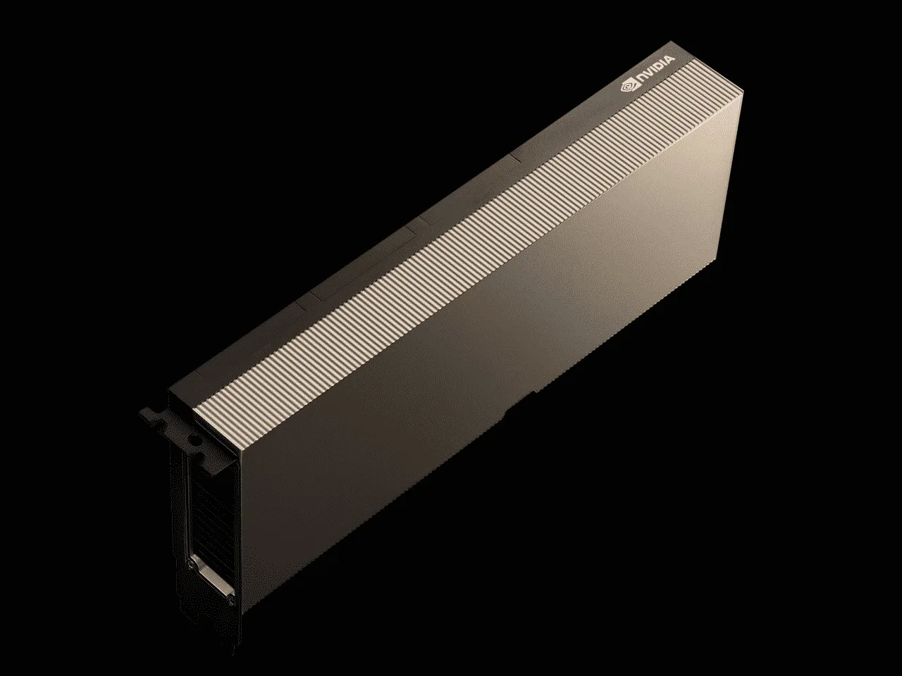
Coming to the specifications, the A100 PCIe GPU accelerator retains the specifications as the 250W variant with 6912 CUDA cores arranged in 108 SM units, 432 Tensor Cores, and 80 GB of HBM2e memory. It has a bandwidth of 2.0 TB/s.
Speaking on the performance side, the FP64 is rated at 9.7/19.5 TFLOPs, FP32 performance is rated at 19.5 /156/312 TFLOPs (Sparsity), FP16 performance is rated at 312/624 TFLOPs (Sparsity), and finally, the INT8 is rated at 624/1248 TOPs (Sparsity). The latest HPC accelerator will be released next week and the price is estimated to be over $20,000 US.
NVIDIA Ampere GA100 GPU Based Tesla A100 Specs:
| NVIDIA Tesla Graphics Card | Tesla K40 (PCI-Express) | Tesla M40 (PCI-Express) | Tesla P100 (PCI-Express) | Tesla P100 (SXM2) | Tesla V100 (SXM2) | Tesla V100S (PCIe) | NVIDIA A100 (SXM4) | NVIDIA A100 (PCIe4) |
| GPU | GK110 (Kepler) | GM200 (Maxwell) | GP100 (Pascal) | GP100 (Pascal) | GV100 (Volta) | GV100 (Volta) | GA100 (Ampere) | GA100 (Ampere) |
| Process Node | 28nm | 28nm | 16nm | 16nm | 12nm | 12nm | 7nm | 7nm |
| Transistors | 7.1 Billion | 8 Billion | 15.3 Billion | 15.3 Billion | 21.1 Billion | 21.1 Billion | 54.2 Billion | 54.2 Billion |
| GPU Die Size | 551 mm2 | 601 mm2 | 610 mm2 | 610 mm2 | 815mm2 | 815mm2 | 826mm2 | 826mm2 |
| SMs | 15 | 24 | 56 | 56 | 80 | 80 | 108 | 108 |
| TPCs | 15 | 24 | 28 | 28 | 40 | 40 | 54 | 54 |
| FP32 CUDA Cores Per SM | 192 | 128 | 64 | 64 | 64 | 64 | 64 | 64 |
| FP64 CUDA Cores / SM | 64 | 4 | 32 | 32 | 32 | 32 | 32 | 32 |
| FP32 CUDA Cores | 2880 | 3072 | 3584 | 3584 | 5120 | 5120 | 6912 | 6912 |
| FP64 CUDA Cores | 960 | 96 | 1792 | 1792 | 2560 | 2560 | 3456 | 3456 |
| Tensor Cores | N/A | N/A | N/A | N/A | 640 | 640 | 432 | 432 |
| Texture Units | 240 | 192 | 224 | 224 | 320 | 320 | 432 | 432 |
| Boost Clock | 875 MHz | 1114 MHz | 1329MHz | 1480 MHz | 1530 MHz | 1601 MHz | 1410 MHz | 1410 MHz |
| TOPs (DNN/AI) | N/A | N/A | N/A | N/A | 125 TOPs | 130 TOPs | 1248 TOPs 2496 TOPs with Sparsity | 1248 TOPs 2496 TOPs with Sparsity |
| FP16 Compute | N/A | N/A | 18.7 TFLOPs | 21.2 TFLOPs | 30.4 TFLOPs | 32.8 TFLOPs | 312 TFLOPs 624 TFLOPs with Sparsity | 312 TFLOPs 624 TFLOPs with Sparsity |
| FP32 Compute | 5.04 TFLOPs | 6.8 TFLOPs | 10.0 TFLOPs | 10.6 TFLOPs | 15.7 TFLOPs | 16.4 TFLOPs | 156 TFLOPs (19.5 TFLOPs standard) | 156 TFLOPs (19.5 TFLOPs standard) |
| FP64 Compute | 1.68 TFLOPs | 0.2 TFLOPs | 4.7 TFLOPs | 5.30 TFLOPs | 7.80 TFLOPs | 8.2 TFLOPs | 19.5 TFLOPs (9.7 TFLOPs standard) | 19.5 TFLOPs (9.7 TFLOPs standard) |
| Memory Interface | 384-bit GDDR5 | 384-bit GDDR5 | 4096-bit HBM2 | 4096-bit HBM2 | 4096-bit HBM2 | 4096-bit HBM2 | 6144-bit HBM2e | 6144-bit HBM2e |
| Memory Size | 12 GB GDDR5 @ 288 GB/s | 24 GB GDDR5 @ 288 GB/s | 16 GB HBM2 @ 732 GB/s 12 GB HBM2 @ 549 GB/s | 16 GB HBM2 @ 732 GB/s | 16 GB HBM2 @ 900 GB/s | 16 GB HBM2 @ 1134 GB/s | Up To 40 GB HBM2 @ 1.6 TB/s Up To 80 GB HBM2 @ 1.6 TB/s | Up To 40 GB HBM2 @ 1.6 TB/s Up To 80 GB HBM2 @ 2.0 TB/s |
| L2 Cache Size | 1536 KB | 3072 KB | 4096 KB | 4096 KB | 6144 KB | 6144 KB | 40960 KB | 40960 KB |
| TDP | 235W | 250W | 250W | 300W | 300W | 250W | 400W | 250W |