For the gaming and consumer segment, NVIDIA GA102 is the largest Ampere GPU. It is used in the high-end graphics cards GeForce RTX 3090 and GeForce RTX 3080. Also, several other products are planned, and in the future, you could see those in both GeForce and Quadro segments.
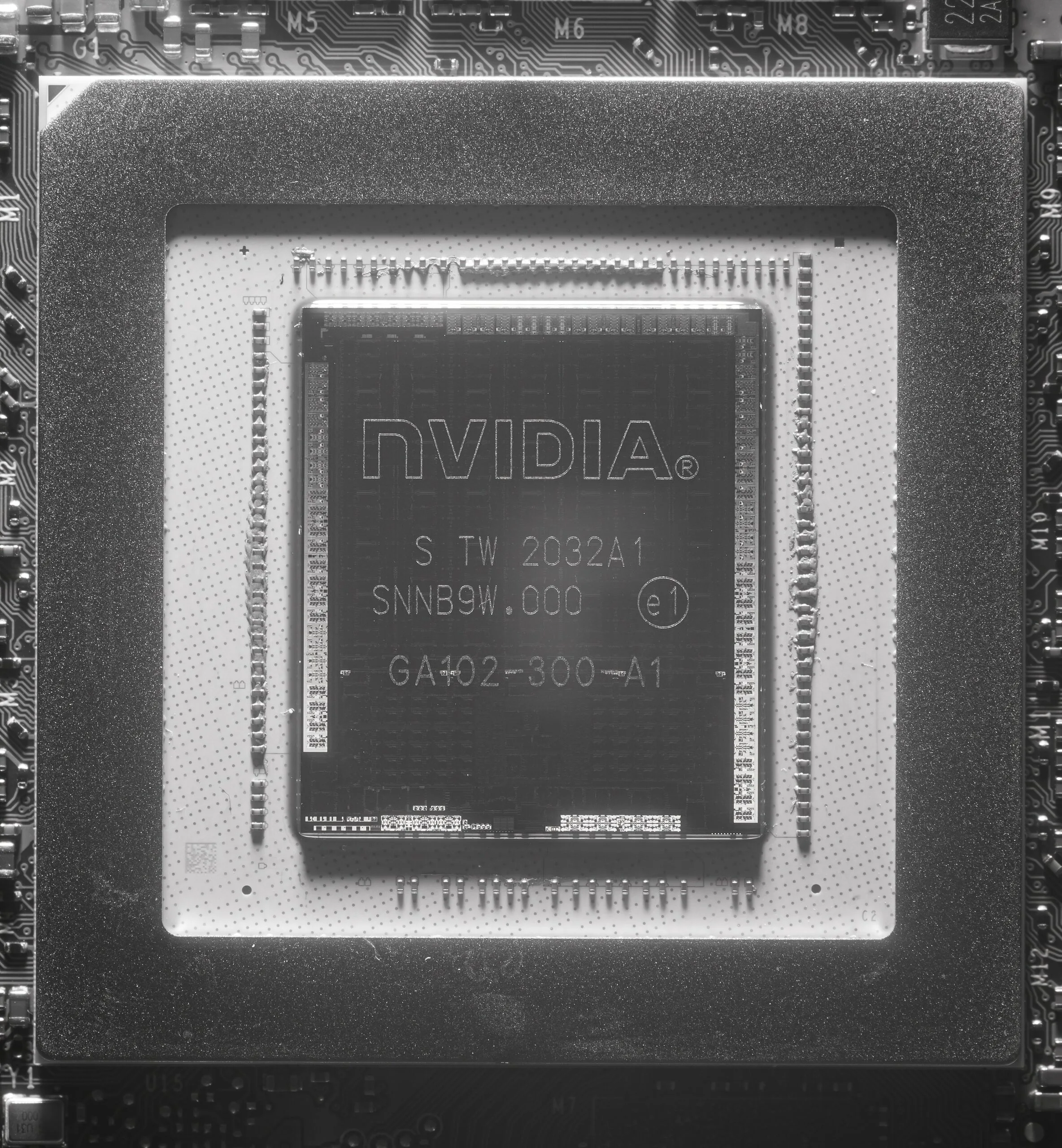
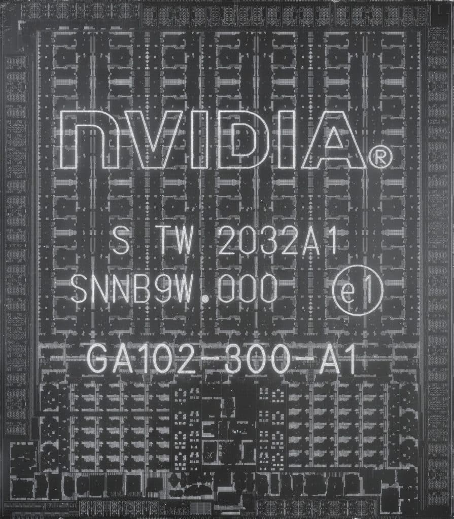
Fritzchens Fritz is popular for taking high-resolution pictures of various GPUs and CPUs, who now reveals the first die shot of the GA102. Fritz’s most recent picture is the Zen 3 die featured on the Ryzen 5000 CPUs, and now we have the clear inside pictures of an Ampere based GeForce RTX series GPUs.
A GeForce RTX 3090 graphics card was used to get these clear shots. The cooler was removed because, in the modern GPUs, the IHS is not used as the previous ones.
Specification of NVIDIA GA102 GPU
The chipset is made with seven graphics processing clusters, and each cluster has 12 SM units. That creates 84 SM units for a total of 10752 cores in a 28.3 billion transistor package. It also features 10 MB of L1, 6 MB of L2 cache, several memory controllers, TMUs, ROPs, and NVLINK HighSpeed I/O hub.
The Ampere SM is divided into four processing blocks, and each of the blocks has 32 FP32 Cores, 16 INT32 Cores, one Tensor Core, one dispatch unit, and one wrap scheduler. Possibly this is made with an updated data path where one data path features 16 FP32 execution units, and the other data path features either 16 FP32 or 16 INT32 execution units.
Locuza shared all the specific parts of the GPU in detail on Twitter, where he always shares various CPU/GPU die shots. Below you can see Locuza’s awesome work where he has done the accurate mapping of the Ampere GA102 GPU.
Fritz and Locuza have done a fine job and now we’ll wait for the same thing with AMD’s Big Navi GPU which is going to be featured on the Radeon RX 6800 and the RX 6900.