During the recent Intel unleashed webcast, Intel’s CEO, Pat Gelsinger, unveiled new details of the 7nm Xe-HPC-based Ponte Vecchio GPU. According to sources, the Intel Ponte Vecchio GPU is first and foremost based on the Xe-HPC graphics architecture which is the flagship product leveraging Intel’s 7nm EUV process node.

The chip also has a ton of other compute tiles that are based on different process nodes, and they merge into one singular exascale graphics processing unit known as Ponte Vecchio. From what we know so far, the GPU primarily makes use of Intel’s 7nm EUV process node but Intel will also be producing some Xe-HPC compute dies through external fabs (such as TSMC).


Raja Koduri teased that there are 7 advanced technologies here, and these would be:
- Intel 7nm
- TSMC 7nm
- Foveros 3D Packaging
- EMIB
- 10nm Enhanced Super Fin
- Rambo Cache
- HBM2
Following is how Intel gets to 47 tiles on the Ponte Vecchio chip:
- 16 Xe HPC (internal/external)
- 8 Rambo (internal)
- 2 Xe Base (internal)
- 11 EMIB (internal)
- 2 Xe Link (external)
- 8 HBM (external)
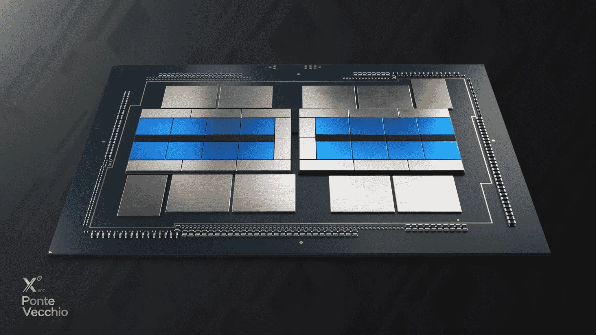
According to reports, the Ponte Vecchio chip is composed of two separate GPU dies, and each die consists of six Xe-HPC Compute units. Each GPU block is attached to four HBM2 stacks which could be either 4-hi or 8-hi. There are eight HBM2 stacks in total and also 8 passive die stiffeners on each GPU. The GPU also makes use of 11 EMIB dies that are featured underneath the HBM2 and I/O link chips.
Here are the actual EU counts of Intel’s various MCM-based Xe HP GPUs along with estimated core counts and TFLOPs:
- Intel Xe HP (12.5) 1-Tile GPU: 512 EU [Est: 4096 Cores, 12.2 TFLOPs assuming 1.5GHz, 150W]
- Intel Xe HP (12.5) 2-Tile GPU: 1024 EUs [Est: 8192 Cores, 20.48 assuming 1.25 GHz, TFLOPs, 300W]
- Intel Xe HP (12.5) 4-Tile GPU: 2048 EUs [Est: 16,384 Cores, 36 TFLOPs assuming 1.1 GHz, 400W/500W]
Intel Xe class GPUs would feature variable vector width as mentioned below:
- SIMT (GPU Style)
- SIMD (CPU Style)
- SIMT + SIMD (Max Performance)