According to UDN, Intel has completed development of its Intel 18A (1.8nm-class) and Intel 20A (2nm-class) fabrication processes, which will be used to produce chips for the company’s own products as well as clients of its Intel Foundry Services (IFS) division.
At an event, Wang Rui, president and chairman of Intel China, announced that the company had completed development of its Intel 18A (18 angstroms-class) and Intel 20A (20 angstroms-class) fabrication processes. This does not imply that the production nodes are ready for commercial production, but rather that Intel has established all specifications, materials, requirements, and performance targets for both technologies.
Intel 20A fabrication technology will use backside power delivery and gate-all-around RibbonFET transistors.
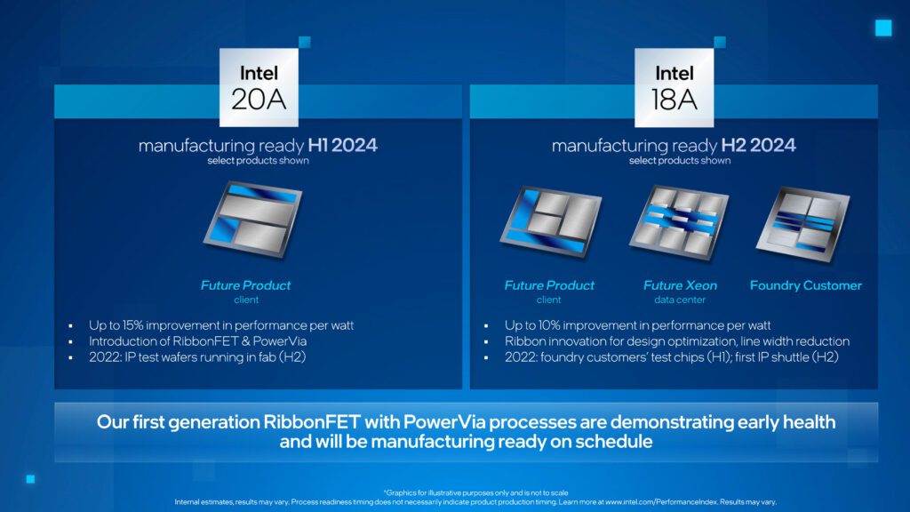
Shrinkage of metal pitches, introduction of all-new transistor structure, and addition of backside power delivery all at the same time is a risky move, but the Intel 20A is expected to allow Intel to leapfrog competitors TSMC and Samsung Foundry. Intel intends to use this node in the first half of 2024.
The Intel 18A manufacturing process from Intel will improve the company’s RibbonFET and PowerVia technologies while also shrinking transistor sizes. This node’s development appears to be going so well that Intel delayed its release from 2025 to the second half of 2024.
Intel had planned to use ASML’s Twinscan EXE scanners with 0.55 NA optics for its 1.8 angstrom node, but because it decided to use the technology sooner, it will have to rely heavily on existing Twinscan NXE scanners with 0.33 NA optics, as well as EUV double patterning.
Also Read: