Huawei has invented (and patented) a chip stacking technology that is expected to be far less expensive than current chip stacking processes. The technology will allow Huawei to continue developing speedier processors using older, more mature production technology, perhaps allowing it to evade US penalties.
The only concern is whether Huawei will be able to capitalise on its breakthrough, considering that foundries are unable to make chips for the company without a US government export licence. But Huawei clearly believes it can, especially since this technology might increase performance for circuits based on older nodes that aren’t subject to the same stringent US limitations.
Huawei can’t access any current node (e.g., TSMC’s N5) since the US government blacklisted Huawei and its chip design company HiSilicon and now requires all companies creating silicon to seek for an export licence because all semiconductor production incorporates technologies created in the US.
According to DigiTimes, Huawei’s former rotating chairman Guo Ping stated at a recent news conference that “innovative chip packaging and chiplet interconnection technologies in general, as well as 3D stacking in particular, are a way for the company to throw in more transistors into its SoCs and get the performance it needs to be competitive.”
Leading-edge processors will require innovative chip packing and multi-chiplet connecting technologies in the next years, therefore all major chip developers and manufacturers already have their own proprietary chip packaging and interconnection methods.
Chipmakers often utilise one of two packaging and interconnection methods: 2.5D packaging, which allows for a high-density/high-bandwidth in-package interconnect for chiplets sitting next to each other, and 3D packaging, which shrinks processors by stacking multiple chiplets on top of one another. However, because chiplets must interact and power must be given via TSVs, 3D packaging often necessitates quite an intricate wiring.
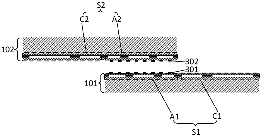
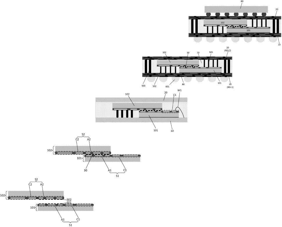
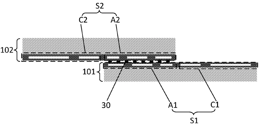
This new technology from Huawei establishes a logical connectivity by overlapping parts of the chiplets
Meanwhile, two or more chiplets each have their own power delivery pins, which are connected to their own redistribution layer (RDL) in a variety of ways. While Huawei’s patented method avoids the use of TSVs, it does not appear to be simple or inexpensive to deploy.
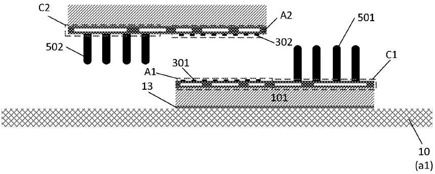
Before connecting to another chiplet, Huawei flips one of the chiplets upside down (or others). It also necessitates the construction of at least two redistribution layers to deliver power (e.g., two chiplets require two RDLs, three chiplets require two RDLs, and four chiplets require four RDLs, as seen in the above gallery), which is not inexpensive due to the additional process steps. The good news is that one of the chips’ redistribution layers can be used to connect items like memory, saving space.
It’s worth noting that Semiconductor Manufacturing International Corp. (SMIC), with whom Huawei is apparently planning to build a fab, is similarly banking on superior packaging and interconnection technologies to circumvent US sanctions. SMIC requires advanced packaging and connecting methods since it does not have access to the production tools required to create semiconductors utilising sub-10nm fabrication technology.
Also read:
The House of the Dead Remake is making its way to PlayStation and Xbox platforms