Following Intel’s Alder Lake launch, AMD details its 3D V-Cache stacking

Obviously, Intel has made a huge announcement of its Alder Lake CPUs sporting up to 16 cores and 24 threads, which has again raised some enthusiasm among geeks and fans. So, AMD had to show what it has next, and it detailed its 3D V-Cache stacking technology, which they first unveiled at the Computex 2021.

  • Following Intel's Alder Lake launch, AMD details its 3D V-Cache stacking
  • Following Intel's Alder Lake launch, AMD details its 3D V-Cache stacking
  • Following Intel's Alder Lake launch, AMD details its 3D V-Cache stacking
  • Following Intel's Alder Lake launch, AMD details its 3D V-Cache stacking
  • Following Intel's Alder Lake launch, AMD details its 3D V-Cache stacking

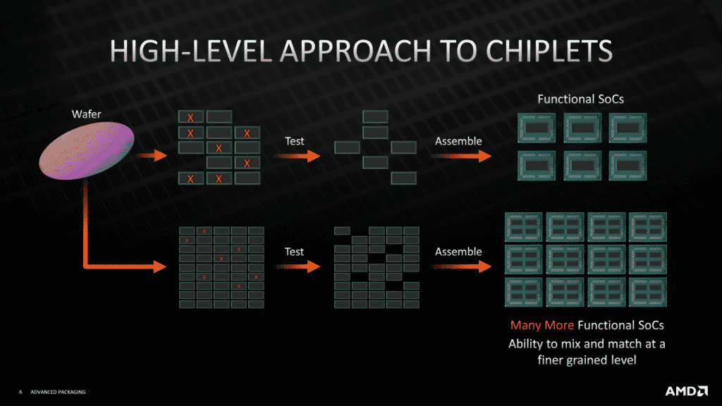
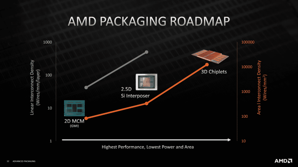
In Hot Chips 33 presentation, AMD also outlined the future of 3D stacking technology and shared the first details on its 3D V-Cache stacking. It demonstrated that the TSV (Through Silicon Via), a vertical inter-wafer or inter-die connection, sees an increase in bonds. The technology will be focusing on more complex 3D stacking designs.

Following Intel's Alder Lake launch, AMD details its 3D V-Cache stacking

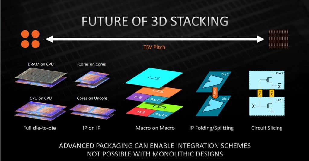
This will enable AMD to stack multiple dies on top of others like DRAM on CPUs or CPUs on CPUs or Cores on Cores and even IP on IP. So, the technology is progressing towards stacking separate modules on each other only to allow macroblocks to be stacked.

Following Intel's Alder Lake launch, AMD details its 3D V-Cache stacking

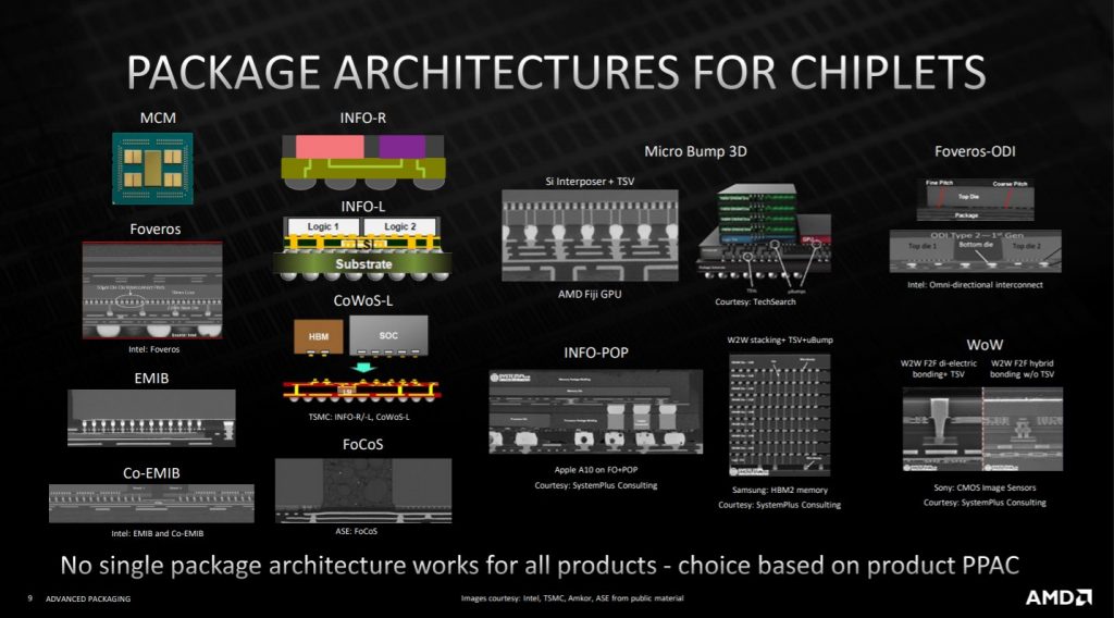
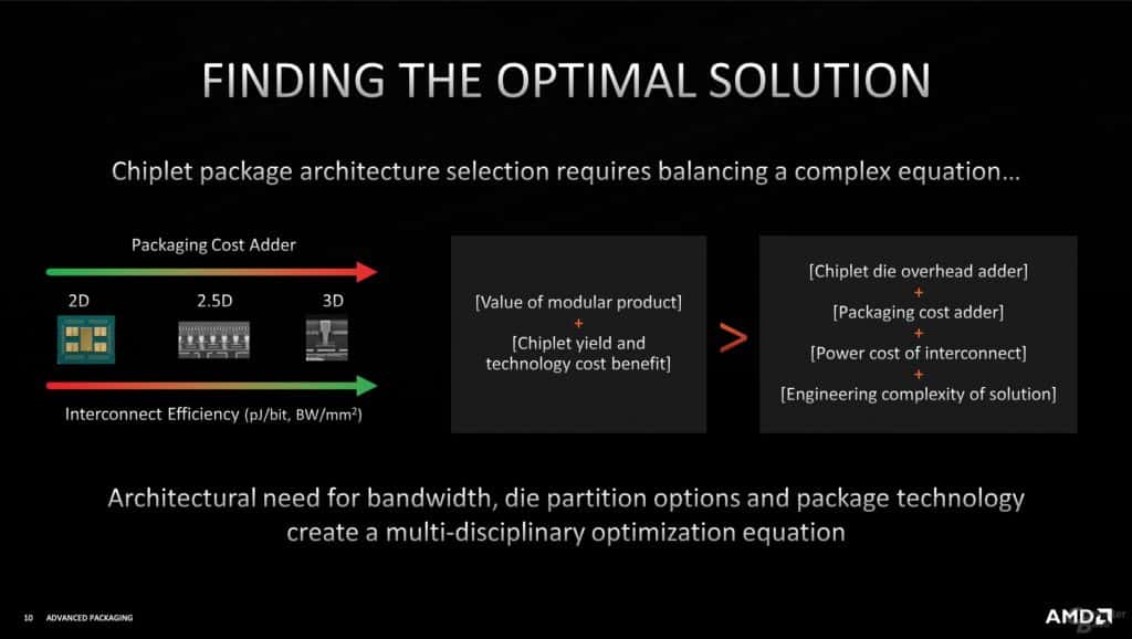
AMD even listed the possibilities of various package architectures as a substitute for 3D V-Cache stacking, including Intel’s Foveros technology. The TSV pitch will be so dense that module splitting or folding or even circuit splitting will be possible; this will completely change the landscape of future processors.

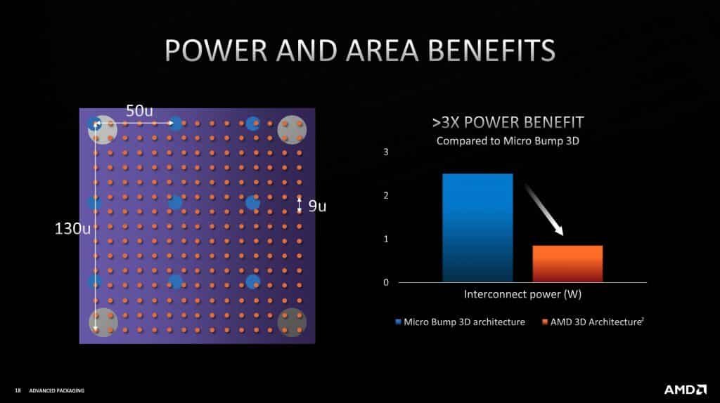
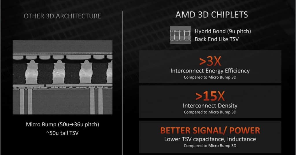
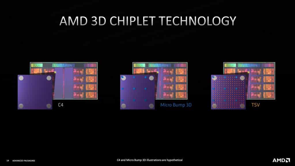
AMD has used a micro bump pitch of 9 microns that is even denser than future Intel Foveros Direct technology at 10 microns. Obviously, you will have efficiency benefits; the interconnect energy efficiency is rated at higher than 3 times compared to Micron Bump 3D.

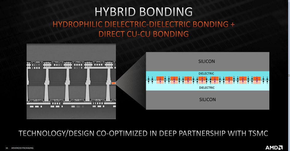
While the interconnect density is rated at more than 15 times higher than Micron Bump 3D, these 3D Chiplets also offer better signal/power thanks to lowering TSV capacitance and inductance. The technology wouldn’t have been possible without TSMC, as it uses a brand new hydrophilic Dielectric-Dielectric Bonding with Direct CU-CU bonding that was designed and co-optimized in deep partnership with TSMC.

  • Following Intel's Alder Lake launch, AMD details its 3D V-Cache stacking
  • Following Intel's Alder Lake launch, AMD details its 3D V-Cache stacking
  • Following Intel's Alder Lake launch, AMD details its 3D V-Cache stacking
  • Following Intel's Alder Lake launch, AMD details its 3D V-Cache stacking
  • Following Intel's Alder Lake launch, AMD details its 3D V-Cache stacking

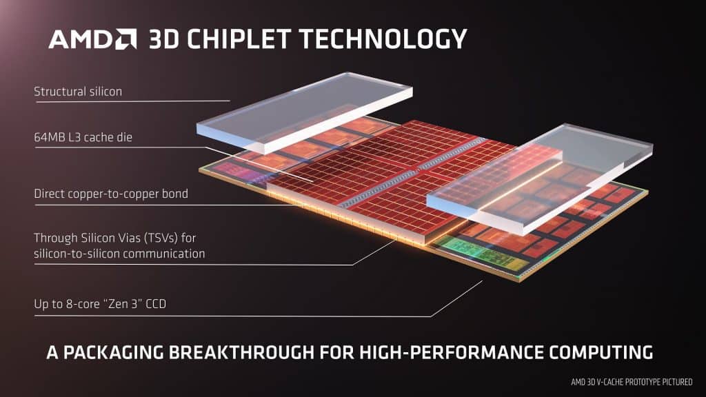
This means two individual silicons (chiplets) can now be bonded together using this technology. AMD also showed stacking 3D chipsets based on AMD’s Zen 3 CPU, featuring silicon to silicon TSV. 

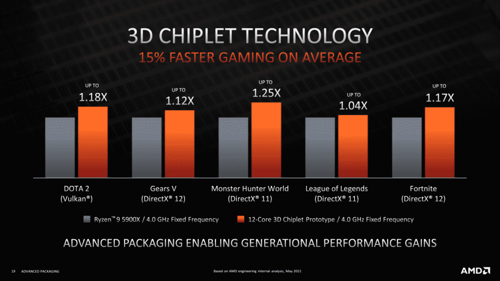
This automatically increases the Level 3 cache by 64MB, and as we remember, AMD showed 3D V-Cache technology in action on its best selling AMD Ryzen 9 5900X CPU with 32+64MB L3 cache. With the change in configuration and new packaging technique, you see an increase in the framerate by 15% on average, which is almost a generational uplift in performance.

Following Intel's Alder Lake launch, AMD details its 3D V-Cache stacking

So, indeed AMD, at Hot Chips 33 presentation, made it clear that if Intel will adopt Hybrid technology, it is also ready with its 3D V-Cache stacking technology and is in the high-performance computing race.

Back at Computex 2021, when the technology was unveiled, AMD also announced that Ryzen CPUs with 3D V-Cache would be mass-produced by the end of this year, so it will be interesting to see when AMD brings them to market to counter Intel.

LEAVE A REPLY

Please enter your comment!
Please enter your name here

This site uses Akismet to reduce spam. Learn how your comment data is processed.

More like this

AMD

AMD Surges Ahead in 2025: Gains 16.6% CPU Market...

In a dramatic shift in the CPU landscape, AMD has pulled off one of its biggest wins...
AMD Ryzen Z2 AI Extreme

AMD Ryzen Z2 AI Extreme: A Game-Changing AI SoC...

AMD Ryzen Z2 AI Extreme: The battle for handheld gaming dominance is heating up — and AMD...
AMD Dominates AI Benchmarks: Instinct GPUs Shatter Records in MLPerf Tests

AMD Dominates AI Benchmarks: Instinct GPUs Shatter Records in...

The AI acceleration race has shifted into high gear, and AMD has just made a spectacular power...
AMD’s ZT Systems Acquisition: Strategic Move to Dominate the $500B AI Data Center Market

AMD’s ZT Systems Acquisition: Strategic Move to Dominate the...

In the high-stakes chess game that is the AI hardware industry, AMD just made a bold queen’s...
AMD Ryzen 9000G APUs

AMD Ryzen 9000G APUs with Zen 5 and RDNA...

AMD Ryzen 9000G APUs : AMD is reportedly gearing up to release its Ryzen 9000G APU...

LATEST NEWS

New Aadhaar App: Face ID and QR Code Features Explained

The new Aadhaar app is set to transform how Indians verify their identity. This blog post delves into the app’s innovative features, focusing on...

Dell Technologies India Unveils Game-Changing AI PC Lineup

The next generation of computing has arrived, and Dell is leading the charge with groundbreaking AI-powered devices designed for every professional need Are you ready...

RBI Repo Rate Cut 2025: What does the Second RBI Monetary Policy Repo Rate Cut Mean for Investors?

The Reserve Bank of India has just delivered a significant monetary policy shift that could reshape investment strategies across the nation. In its April...

NYT Wordle April 9, 2025: Today’s Answer, Hints, and Strategy Guide (1390)

In the ever-evolving landscape of daily brain teasers, NYT Wordle continues to reign supreme as the most beloved word puzzle that unites millions of...

Featured