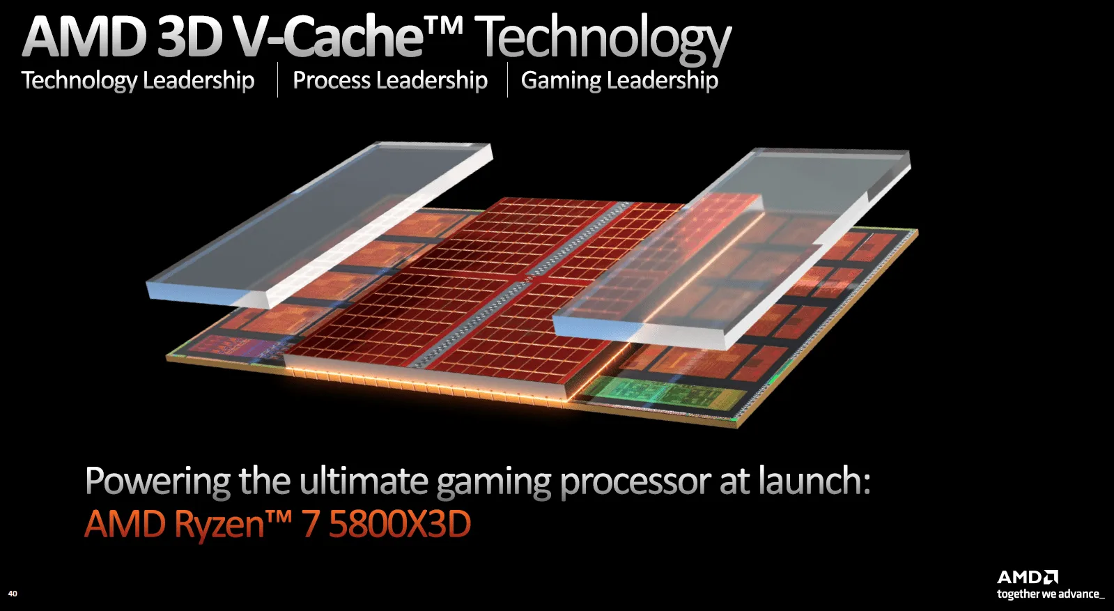
The AMD Ryzen 7000X3D lineup, which includes the Ryzen 9 7900X3D, Ryzen 9 7950X3D, and Ryzen 7 7800X3D, is one of the world’s fastest gaming processors. AMD accomplished this feat thanks to its proprietary 3D V-Cache technology. AMD has also been working on improving its 3D chip stacking design and is now ready to reveal information about its new second-generation 3D V-Cache chiplet design.
The second-generation 3D V-Cache chiplet design employs the same 7nm manufacturing process as its predecessor but has a higher bandwidth of 2.5 TB/s as opposed to 2 TB/s. Moving forward with the second-generation 3D V-Cache design using the less expensive and now mature 7nm manufacturing process. The company is now investigating ways to improve performance while lowering costs.
AMD is also the sole manufacturer of 3D V-Cache chips, with no competition from Intel, making them the fastest in gaming and specific applications.
AMD had to stack an additional L3 SRAM chiplet directly in the centre of the Zen 3 compute die or (CCD) to isolate the 3D V-Cache chiplet from the heat generation cores. This added 96 MB of cache to Zen 3 chips, making it the fastest chip in latency-sensitive processes like gaming and applications.
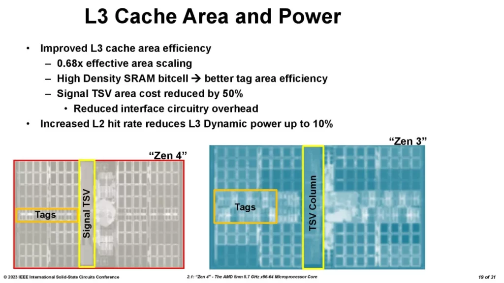
AMD had to make some changes because Zen 4 chips used a new and smaller 5nm manufacturing process, whereas its 3D V-Cache chiplet remained based on the 7nm manufacturing process. AMD chose a smaller 7nm SRAM die, measuring only 36mm2 versus 41mm2 on the Zen 3 chips. In addition, the total number of transistors remained constant at 4.7 billion.
This resulted in a 25% increase in bandwidth to 2.5 TB/s, making the same 7nm chiplet design denser than the Zen 4 5nm compute chiplet and 3x denser than the Zen 3 7nm compute chiplet.
Also Read: