In recent news, the Advanced Micro Devices company has recently posted a new patent. According to the patent, the company is working on a new chip-let that acts as a bridge between multiple GPU dies, possibly based on its next-generation RDNA 3 architecture for GPUs and APUs.
AMD has, for many years been criticizing the conventional monolithic GPU designs. AMD has already implemented the chip-let design in its CPU segment & the company is now planning to follow the same route on the GPU side.
Not only that but AMD’s rival, NVIDIA, is also investing in MCM designs that will be utilized in its next-generation GPUs. Both the rivals are looking for an advancement in their GPU technologies as there is a growing demand for high-performance GPUs.
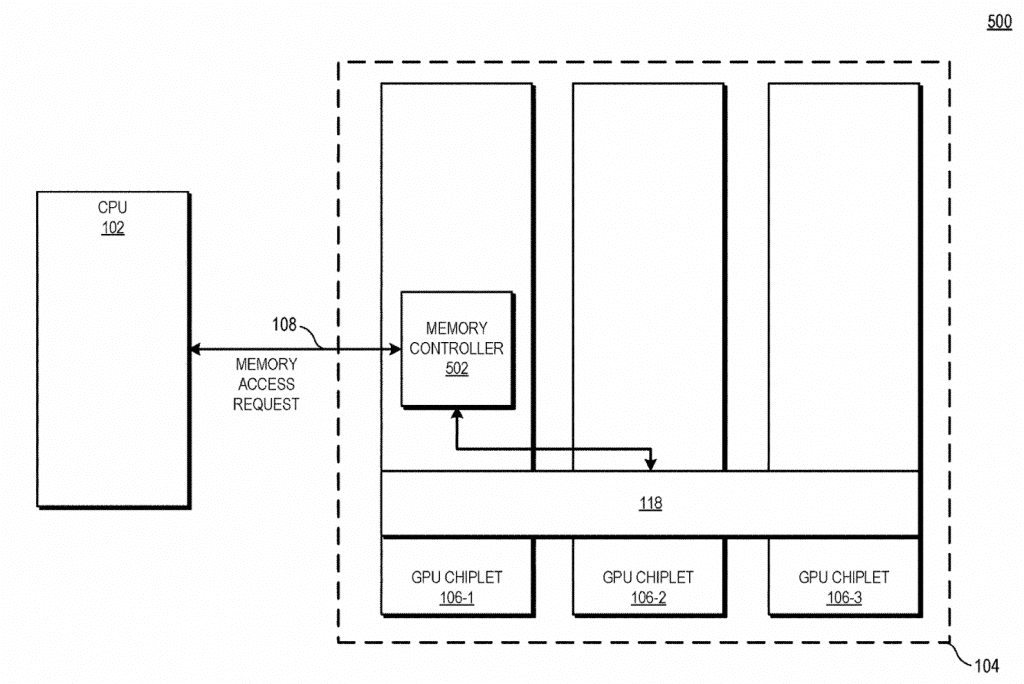
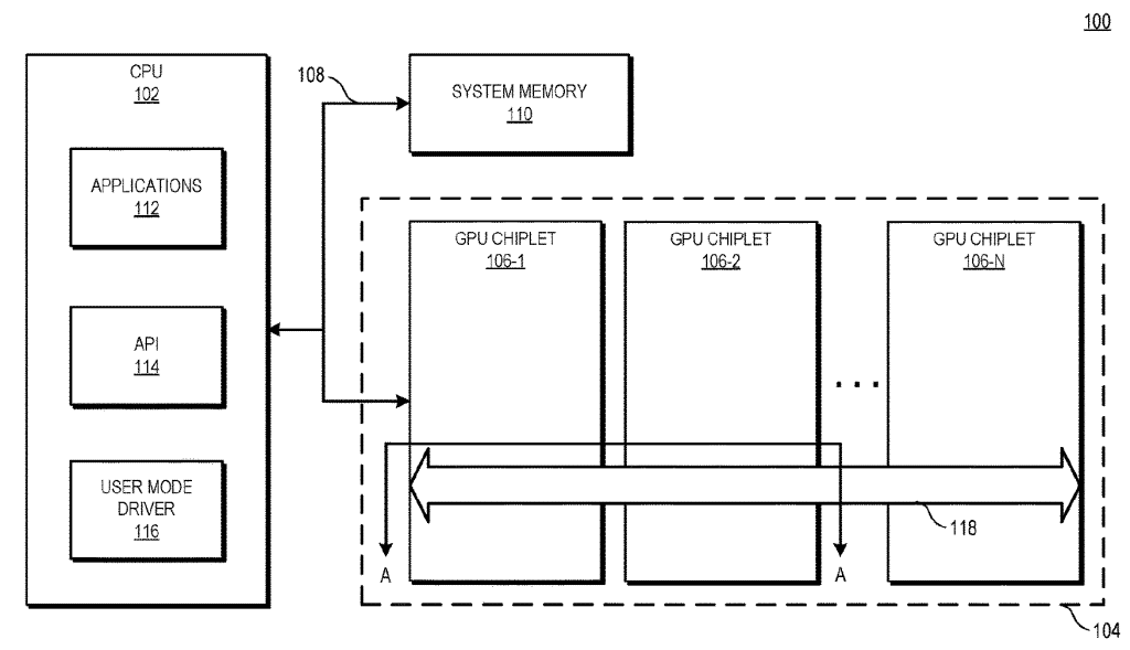
In the case of AMD, sources indicate that the chipmaker has plans to invest heavily in chip-let designs for its next-generation GPU architectures. However, the chipmaker has stated that it faces a problem in making multiple GPUs work in parallel, think of Crossfire which is a redundant technology as are all multi-GPU implementations. To fix this problem, AMD has proposed an active bridge chipset that would bridge multiple GPU chipsets together.
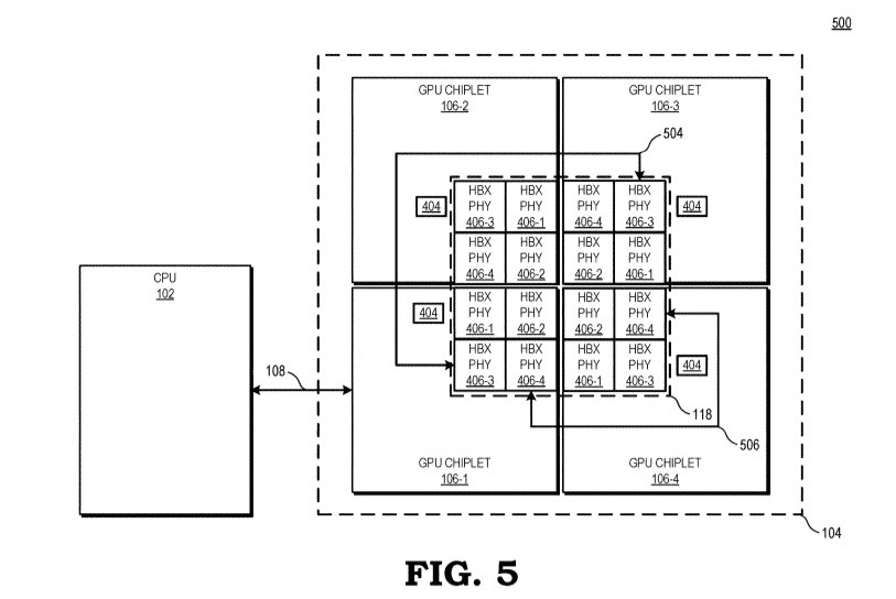
The block diagram filed in the patent shows a chip featuring multiple chipsets, and the CPU portion is connected to the first GPU chipset via a communication bus (future generation of Infinity Fabric) while the GPU chipsets are interconnected via the active bridge chipset.
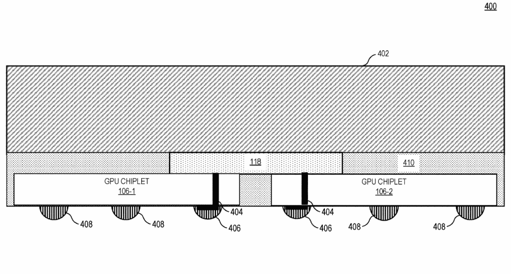
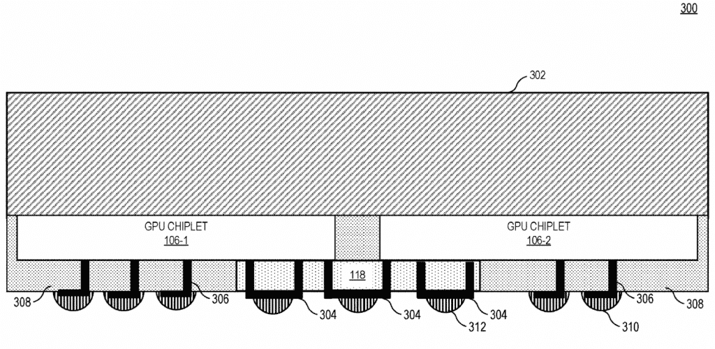
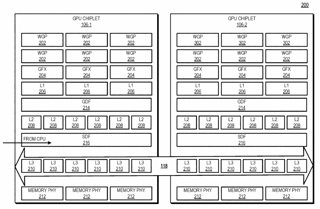
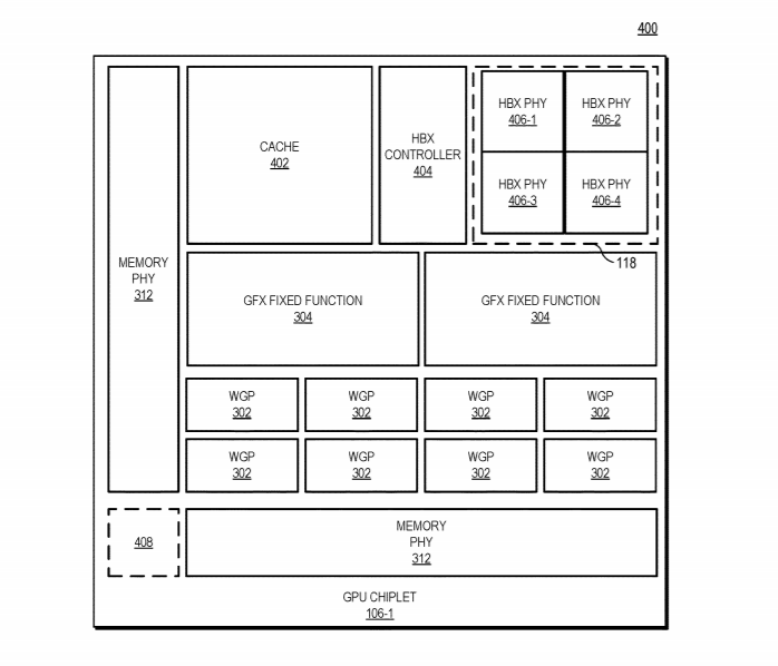
The bridge will also feature an L3 LLC (Last Level Cache) which is coherent and unified across the multiple chipsets and reduce cache bottlenecks. The block diagram indicates that there might be a design also ready for the future AMD RDNA 3 based APUs.