Moore’s Law is Dead has obtained brand-fresh images of AMD’s Navi 32 GPU package, which houses a Navi 31 RDNA 3 GPU die. AMD’s Navi 32 GPU was accidentally disclosed in a Forbes video that revealed a somewhat smaller GPU package housing the Navi 32 GCD and four MCDs. We now have new images of the identical package, but instead of the Navi 32 design, the chip now houses a Navi 31 GPU.
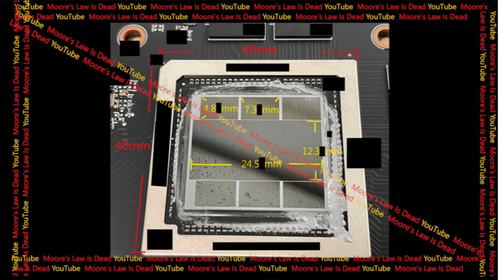
The AMD Navi 31 GPU is housed in the same packaging shown in the Navi 32 GPU leak, according to an image published by Moore’s Law is Dead.
The Navi 31 GCD, which measures 304.35mm2, and the six MCDs for a 529mm2 die size can be seen in the middle. The biggest change is that the Navi 31 GPU is housed in a significantly smaller box measuring only 40x40mm, as opposed to the conventional Navi 31 package of 55×47.5mm2.
The next stage is to create hardware-protected qubits, and Svore stated that the team is making significant progress in this regard. These qubits will be tiny (less than 10 microns on a side) and fast enough to perform a single qubit operation in under a microsecond. Following that, the team intends to work on entangling these qubits and operating them via a process known as braiding, which has been explored (mainly as a theory) since at least the early 2000s.
According to MLID, AMD supplied Navi 31 RDNA 3 GPU dies in Navi 32 packages to its partners for thermal testing before Navi 32 was even ready. The GPU also includes two dummy MCD dies, implying that the Navi 31 GPU is essentially a 256-bit bus design rather than the full 384-bit or even the reduced 320-bit architecture found in the 7900 XT. In terms of design, this chip may be extremely similar to the Radeon Pro W7800, but it, too, uses the normal Navi 31 packaging, albeit with two MCD dies disabled.
We believe the card will include at least eight GDDR6 dies, allowing for a 256-bit bus interface and 16 GB of VRAM. Why is this Navi 31 package interesting? Because a similar die can be used for high-end laptop GPUs in the future.
Also read: