
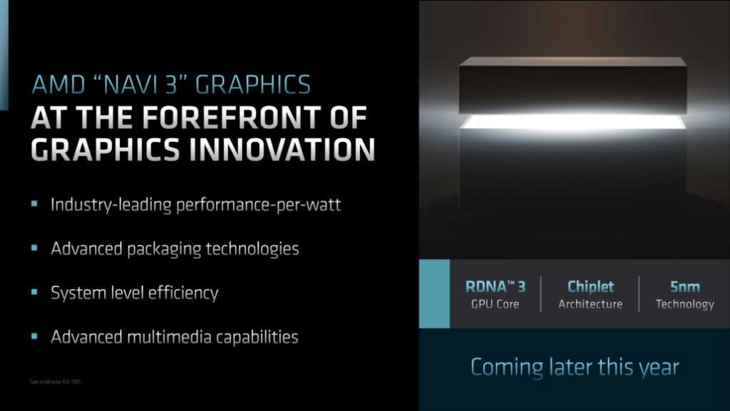
The Navi 31, the reported flagship AMD GPU for the forthcoming RDNA 3 generation and a product of TSMC’s 5nm production node, has been given die size. Greymon55, who released the purported die size of the next-generation GPU powerhouse from camp red, is the source of the rumors. The following are some of the major RDNA 3 GPU characteristics that AMD will emphasize:
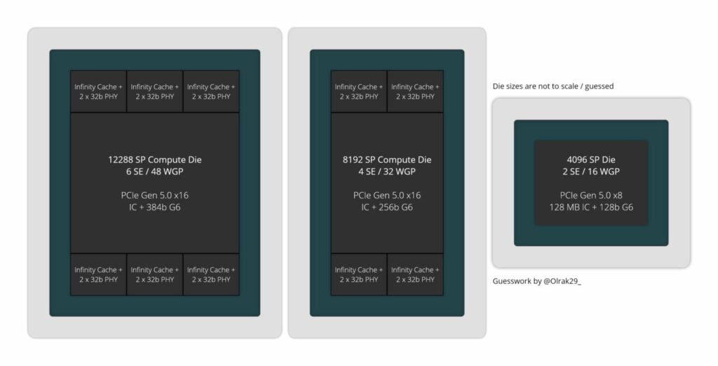
The AMD RDNA 3 GPU was rumored to have a total die area of 600 mm2, but the real GPU die size would be nearly half that. The entire die package will include both the cache “MCDs” and the GPU “GCD,” which is the reason for this. According to the earlier speculation, the top-tier Navi 31 GPU will have a total of six RDNA 3 MCDs. Although they will be fused into one package, each MCD will be independent of the GCD. The RDNA 3 Navi 31 GCD will have a lower die size, roughly 350mm2.
With a die size of 520mm2, the AMD Navi 21 RDNA 2 GPU would experience a 33 percent size reduction using the TSMC 5nm production node.
On the other hand, the MCDs are anticipated to be produced on TSMC’s 6nm process node. The staff at 3DCenter have done an intriguing comparison, stating that the Navi 21 GPU will end up having a die size of about 375mm2 without the Infinity Cache & memory controllers. That makes it quite comparable to the Navi 31 GPU, but the new flagship has more than twice as many cores. If the new chip were to be built on the older 7nm node, the GPU die might be larger than 500 mm2.
Additionally, @Kepler L2 notes that to save space, the RDNA 3 GPU architecture used in the Navi 31 SKU has eliminated many on-die technologies like XGMI, GDS (Global Data Share), the Legacy Geometry Pipeline, and Legacy Scan Converter. Since the RDNA 3 GPUs do not have certain GPU capabilities, likely, they are not necessary.
The Radeon RX 7900 XT graphics card and other next-generation enthusiast cards would be powered by AMD Navi 31 GPU, the top-tier RDNA 3 processor. We’ve heard that AMD would replace its next-generation RDNA 3 GPUs’ compute units with workgroup processors. Dual CU (Compute Units) will be housed in each WGP, but there will be four SIMD32 clusters per CU, as opposed to two on each CU in RDNA 2. According to rumors, AMD has the choice of the 6nm die from TSMC or Samsung.
The AMD Navi 31 GPU with RDNA 3 architecture is anticipated to feature a single GCD with 48 GPS, 12 SAs, and 6 SEs, according to the most recent information. This will distribute 12,288 stream processors in total, which is fewer than the prior tally. This will reduce total computing performance as well until AMD overclocks its flagship part to over 3.0 GHz. The Navi 31 GPU will also include 6 MCDs, each of which will have a 64 MB Infinity Cache and maybe also the 64-bit (32-bit x 2) memory controllers, giving the device a 384-bit bus interface.
When it debuts later this year, the AMD Navi 31 GPU will face off against the purported 600W and 600mm2 NVIDIA AD102 GPU that makes use of the Ada Lovelace graphics architecture.
also read:
AMD EPYC 9654 Genoa 96 Core monster Benchmarked in Latest Cache and Memory tests