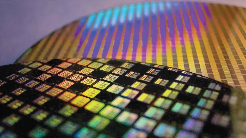
The semiconductor industry is on the brink of another revolution, and Taiwan Semiconductor Manufacturing Company (TSMC) is leading the charge. Already the world’s largest foundry, TSMC is now accelerating efforts to achieve mass production of the cutting-edge 1nm process by the end of the decade. This bold move solidifies Taiwan’s position as a global semiconductor powerhouse and pushes the boundaries of Moore’s Law further than ever before.
Table of Contents
TSMC’s Vision: Bringing 1nm to Reality by 2030
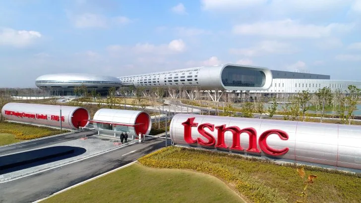
As demand for advanced semiconductor technology surges—fueled by AI, 5G, and high-performance computing—TSMC remains at the forefront of innovation. According to reports from the Taiwan Economic Daily, the company is laying the groundwork for 1nm production with a state-of-the-art facility in Tainan, Taiwan, dubbed “Fab 25.”
This advanced fab will feature six production lines dedicated to manufacturing 12-inch wafers, marking a historic leap in semiconductor miniaturization. TSMC has also confirmed that new facilities for 2nm and 1.4nm (A14 and A10 nodes) will be established in the same region, leveraging government incentives and Tainan’s growing reputation as Taiwan’s own “Silicon Valley.”
Why TSMC’s 1nm Node Is a Game Changer
During the IEDM (International Electron Devices Meeting) conference, TSMC outlined its vision for the future of semiconductor manufacturing. The highlight? The ability to integrate trillions of transistors into a single chip using advanced 3D stacking technology. This breakthrough not only enhances computing power but also sets new industry standards for efficiency and performance.
The significance of this advancement cannot be overstated. As transistor sizes shrink, power efficiency improves, heat generation decreases, and computing speeds skyrocket. This makes 1nm chips ideal for AI-driven applications, quantum computing, and next-generation consumer electronics.
Challenges on the Road to 1nm
Despite TSMC’s ambitious roadmap, achieving 1nm mass production won’t be without its challenges. The semiconductor industry has faced yield issues and supply chain disruptions due to increasing process complexity. Each generational leap requires billions of dollars in R&D and meticulous refinement to maintain high yield rates.
Early estimates suggested that the cost of developing TSMC’s 1nm process would exceed one trillion won (approximately $32 billion)—a figure that has likely risen due to inflation and supply chain constraints. However, with five years to fine-tune its process, TSMC remains confident in its ability to overcome these hurdles.
Taiwan’s Strategic Role in Semiconductor Leadership
TSMC’s dominance in the semiconductor space continues to widen, especially following its acquisition of a majority of NVIDIA’s AI chip orders. This puts competitors like Samsung Foundry and Intel Foundry in a tough position, struggling to close the gap.
By investing heavily in Taiwan’s semiconductor ecosystem, TSMC is reinforcing the country’s global leadership in chip manufacturing. The government’s strong support, along with strategic investments in R&D, talent development, and infrastructure, will play a crucial role in ensuring that Taiwan remains at the epicenter of technological innovation.
What’s Next for TSMC?
With construction set to begin next month on its first European fab in Germany, and expansion plans across the U.S. and Japan, TSMC is rapidly growing its global footprint. However, Taiwan will remain the heart of its most advanced research and development efforts.
As we approach 2030, all eyes will be on TSMC to see if it can pull off one of the biggest technological feats in modern history—ushering in the era of 1nm semiconductors. If successful, this could redefine computing as we know it, powering everything from AI supercomputers to next-gen smartphones and beyond.
Stay tuned for more updates on TSMC’s cutting-edge developments as they continue to push the limits of what’s possible in semiconductor manufacturing.