
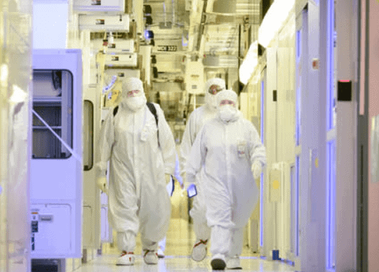
On Wednesday, Intel made a significant announcement regarding the commencement of operations at Fab 9, located in Rio Rancho, New Mexico. This state-of-the-art production facility, boasting a staggering $3.5 billion investment, was purposefully constructed for the packaging of chips utilizing Foveros 3D technology. It stands as one of Intel’s premier fabs exclusively dedicated to advanced packaging technologies, marking a pivotal milestone in the company’s technological evolution.

More About Intel Foveros 3D Chip Facility
Keyvan Esfarjani, Intel’s executive vice president and chief global operations officer, expressed enthusiasm about this milestone, emphasizing the significance of Fab 9 in Intel’s operations. Esfarjani highlighted the groundbreaking nature of this technology, underlining its ability to provide Intel’s customers with unparalleled advantages in performance, form factor, and design flexibility. Moreover, he lauded the collaborative efforts of the New Mexico team, Intel’s broader workforce, suppliers, and contractor partners, recognizing their relentless pursuit of packaging innovation.
Intel’s utilization of Foveros 3D technology extends beyond mere chip packaging; it serves as the foundation for its latest Core Ultra ‘Meteor Lake‘ processors catering to client applications and Ponte Vecchio GPUs designed for artificial intelligence (AI) and high-performance computing (HPC) tasks. As Intel and its customers, particularly those engaged with Intel Foundry Services, increasingly adopt multi-chiplet designs, the demand for Foveros 3D is expected to soar in the coming years.
The current iteration of Intel’s Foveros 3D technology revolves around a 600mm^2 interposer fabricated using its 22FFL process technology. This interposer acts as both an interconnect and a power delivery base die for stacked chiplets. Presently, Foveros 3D boasts 36-micron bump pitches, supporting up to 770 microbumps per square millimeter and achieving up to 160 GB/s per mm bandwidth.
However, Intel envisions significant enhancements in the technology’s interconnection densities with the adoption of 25-micron and 18-micron micro bumps in the future. Furthermore, Intel’s Co-EMIB technology enables the interconnection of multiple Foveros 3D interposers, facilitating the construction of ultra-large data center-grade devices.