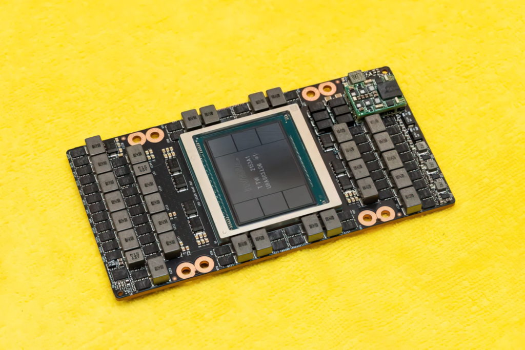
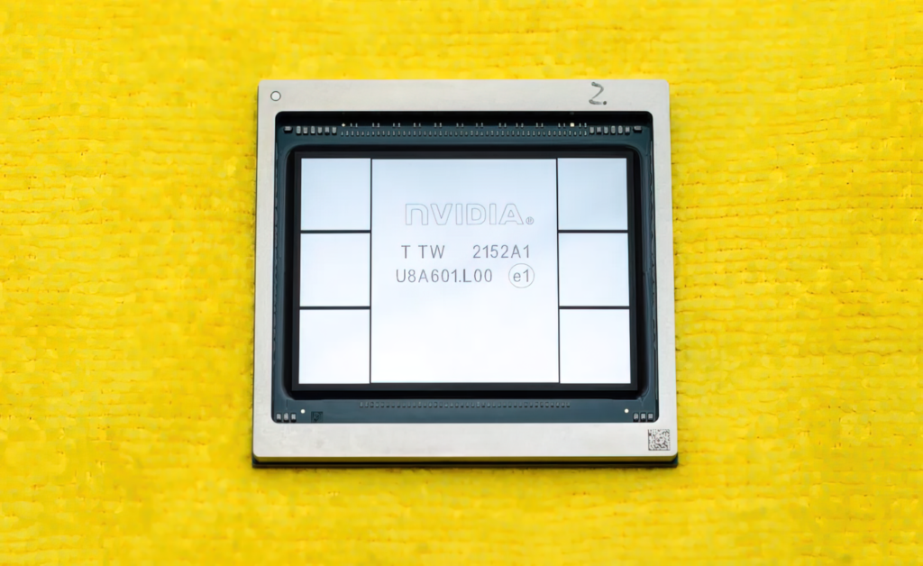
NVIDIA’s Hopper H100 GPU, a computational powerhouse geared for the next generation of data centers, was announced at GTC 2022. CNET obtained not only the graphics board on which the H100 GPU is installed but also the H100 chip. The H100 GPU is a massive device featuring the newest 4nm technology and 80 billion transistors, as well as the cutting-edge HBM3 memory technology.
The H100 is based on the PG520 PCB board, which features over 30 power VRMs and a huge integrated interposer that employs TSMC’s CoWoS technology to combine the Hopper H100 GPU with a 6-stack HBM3 architecture, according to the the the tech outlet.
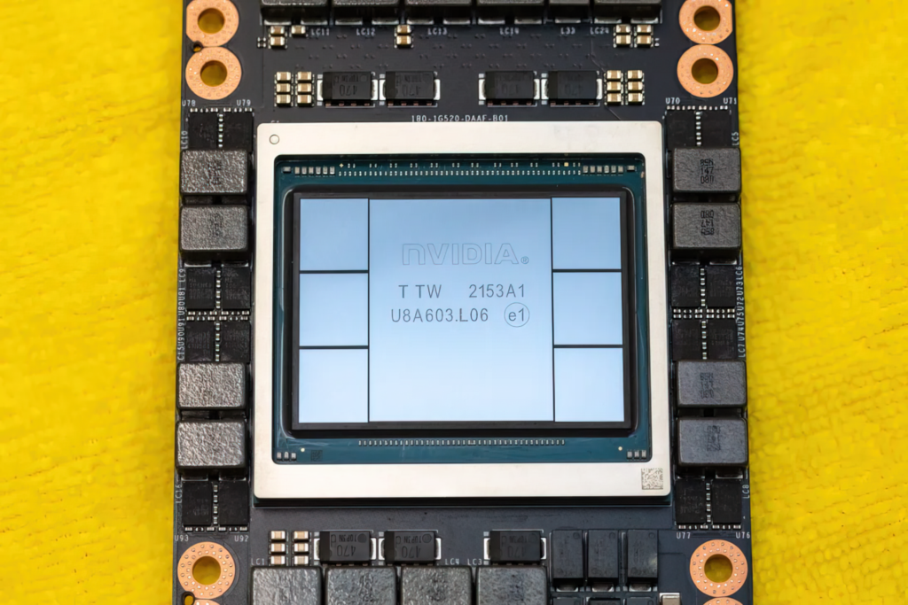
Two stacks are kept out of the six to assure yield integrity. However, the new HBM3 standard enables capacities of up to 80 GB at 3 TB/s, which is incredible. The current fastest gaming graphics card, the RTX 3090 Ti, has just 1 TB/s of bandwidth and 24 GB of VRAM. Aside from that, the H100 Hopper GPU supports the latest FP8 data format, as well as the 700W power architecture that the chip is built around, thanks to its new SXM connector.
In terms of technical specs, the NVIDIA Hopper GH100 GPU is made up of a large 144 SM (Streaming Multiprocessor) chip arrangement that is divided into 8 GPCs. These GPCs contain a total of 9 TPCs, each of which has two SM units. This results in 18 SMs per GPC and 144 SMs for the entire 8 GPC arrangement. Each SM is made up of up to 128 FP32 units, giving us a total of 18,432 CUDA cores. The following are some of the possible configurations for the H100 chip:
- 8 GPCs, 72 TPCs (9 TPCs/GPC), 2 SMs/TPC, 144 SMs per full GPU
- 128 FP32 CUDA Cores per SM, 18432 FP32 CUDA Cores per full GPU
- 4 Fourth-Generation Tensor Cores per SM, 576 per full GPU
- 6 HBM3 or HBM2e stacks, 12 512-bit Memory Controllers
- 60 MB L2 Cache
- Fourth-Generation NVLink and PCIe Gen 5
The NVIDIA H100 GPU with SXM5 board form-factor includes the following units:
- 8 GPCs, 66 TPCs, 2 SMs/TPC, 132 SMs per GPU
- 128 FP32 CUDA Cores per SM, 16896 FP32 CUDA Cores per GPU
- 4 Fourth-generation Tensor Cores per SM, 528 per GPU
- 80 GB HBM3, 5 HBM3 stacks, 10 512-bit Memory Controllers
- 50 MB L2 Cache
- Fourth-Generation NVLink and PCIe Gen 5
Hopper H100 offers a 2.25x improvement over the entire GA100 GPU setup
NVIDIA’s Hopper GPU also has additional FP64, FP16, and Tensor cores, which will significantly improve performance. And that will be required to compete with Intel’s Ponte Vecchio, which is also slated to provide 1:1 FP64.
NVIDIA has paid special attention to the cache in the Hopper GH100 GPU, increasing it to 48 MB. This is a 20% improvement over the Ampere GA100 GPU’s 50 MB cache and three times the size of AMD’s flagship Aldebaran MCM GPU, the MI250X.
The NVIDIA GH100 Hopper GPU will have a compute performance of 4000 TFLOPs in FP8, 2000 TFLOPs in FP16, 1000 TFLOPs in TF32, and 60 TFLOPs in FP64. These staggering numbers obliterate all previous high-performance computing accelerators.
In the FP64 compute, this is 3.3 times faster than NVIDIA’s own A100 GPU and 28% faster than AMD’s Instinct MI250X. The H100 GPU is 3x quicker than the A100 and 5.2x faster than the MI250X in FP16 computation.
also read:
Huawei opts to use the CPUs of Phytium another Blacklisted company for its New Desktop PC
source