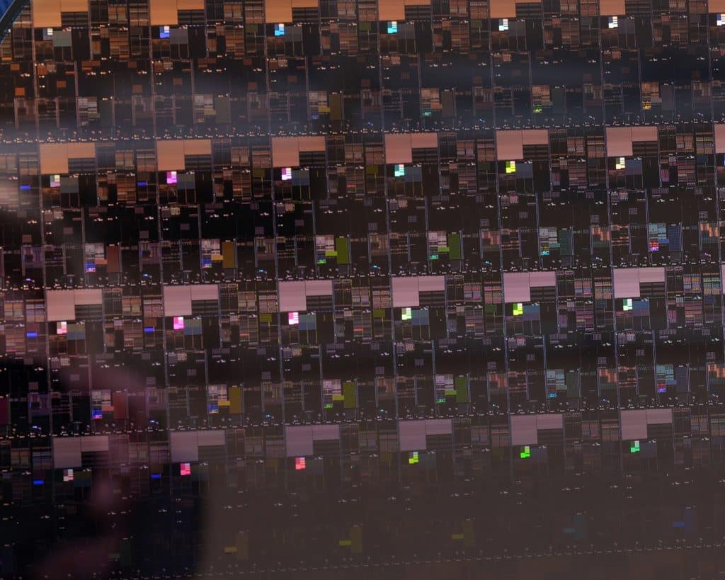
Samsung and IBM announced during their discussion on “3D at the Device Level” at the 67th International Electron Devices Meeting, held this year in San Francisco, CA, that the two tech companies had collaborated to achieve a breakthrough in design techniques for next-generation semiconductor chips. This new technology allows transistors to be stacked vertically, resulting in increased power efficiency or higher performance.
During the presentation, the two companies demonstrated how they could reduce the size of semiconductor chips while also increasing their power and efficiency by redirecting current flow from horizontal to vertical.

CMOS transistors are built in a lateral, or horizontal, fashion, and countless advances over decades have shrunk their dimensions so that billions of them can now be put on a chip, following the predictions of Moore’s Law. But shrinking transistors further to boost chip performance and add new features is difficult and costly. Would orienting them vertically instead of horizontally save space and make it easier to extend the life of Moore’s Law? Inspired by trench-based DRAM vertical access transistors, a team from IBM and Samsung will describe how they turned transistor architecture on its side, with CMOS devices built using so-called Vertical-Transport Nanosheets (VTFETs) on bulk silicon and with a 45nm gate pitch.
— Paper #26.1, “Vertical-Transport Nanosheet Technology for CMOS Scaling beyond Lateral-Transport Devices,” H. Jagannathan et al, IBM/Samsung
Previously, semiconductor chips were laid flat on the silicon’s surface, with the current flowing horizontally. This new design allows the transistors to be perpendicular to the semiconductor chip’s surface rather than parallel. The new technology will allow manufacturers to bypass Moore’s Law’s performance limitations, allowing them to save energy due to low power consumption.
Vertical Transport Field-Effect Transistors, or VTFETs, are a joint effort by Samsung and IBM to vertically stack transistors for improved efficiency and performance. When compared to the current FinFET structure design, the collaboration between the two companies is expected to provide twice the performance, or up to an 85 percent increase in power efficiency. Cryptocurrency miners will see an increase in power efficiency, and the environment’s impact will essentially improve as well.
There’s no word on when the new VTFET technology will be available in commercial products. Intel, along with other tech giants, is rumoured to be working on new angstrom-scale chips, with Intel estimating a release date in the fourth quarter of 2024 under the Intel 20A moniker.
also read:
AMD stock reports steady growth after a decline over the second half of this year


