Union Minister Ashwini Vaishnaw unveiled India’s semiconductor roadmap at the World Economic Forum in Davos on January 21, 2026, announcing plans to produce 7-nanometer chips by 2030 and advance to 3-nanometer technology by 2032. In collaboration with IBM and industry partners, India will first master 28nm-90nm manufacturing—which accounts for 75% of global chip demand—before progressing to advanced nodes, targeting top-five global semiconductor nation status.

India’s Semiconductor Manufacturing Roadmap
| Milestone | Timeline | Focus Applications |
|---|---|---|
| First Indigenous Wafer | FY 2027-28 (Tata Dholera facility) | Foundation building |
| 28nm – 90nm Mastery | 2026-2030 | EVs, automobiles, railways, defense, telecom |
| 7nm Technology | By 2030 | Advanced consumer electronics, AI chips |
| 3nm Technology | By 2032 | Cutting-edge processors, flagship smartphones |
| Partner | IBM + industry ecosystem | Technology transfer, talent development |
| Current Jobs | 25 lakh in electronics manufacturing | Growing to millions more |
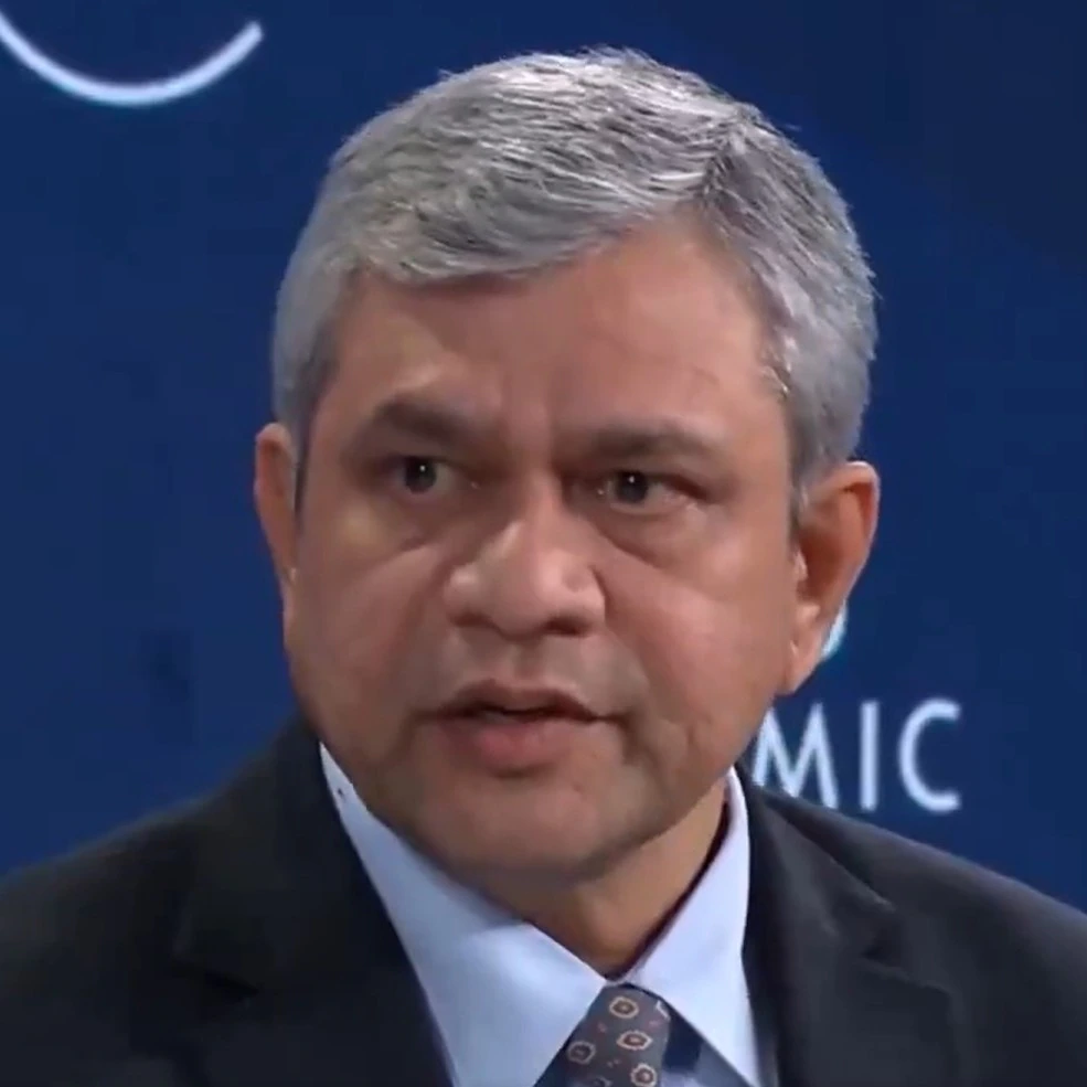
75% of Global Chip Demand Lives in 28nm-90nm Range
Vaishnaw emphasized that nearly 75% of global chip demand lies in the 28nm to 90nm range, serving electric vehicles, automobiles, railways, defense, telecom equipment, and consumer electronics. India prioritizes mastering this segment before advancing to smaller nodes, with IBM CEO Arvind Krishna endorsing the phased approach as “necessary and strategically sound” during NDTV’s Davos dialogue.
For semiconductor industry watchers, the “empty nail” in Vaishnaw’s office symbolizes India’s first indigenous wafer production at Tata’s Dholera facility in FY 2027-28—a concrete timeline signaling serious commitment beyond policy announcements.
IBM Partnership Strengthens Chip Technology and Talent Pool
Vaishnaw met IBM CEO Arvind Krishna at WEF, with collaboration strengthening India’s efforts in advanced chip technology including 7nm and 2nm while developing the semiconductor talent pool. India now has 24 startups designing semiconductor chips, with 18 already securing venture capital funding—demonstrating investor confidence in deep-tech potential.
Krishna cautioned that semiconductor manufacturing doesn’t allow countries to leapfrog stages easily, noting even at 28 nanometers, manufacturers must place billions of transistors with near-perfect precision. He pointed out China hasn’t consistently reached the most advanced end despite decades of investment, validating India’s step-by-step strategy.

Four Semiconductor Plants Begin Production in 2026
Vaishnaw stated four semiconductor plants will start commercial production in 2026, with electronics manufacturing already supporting 25 lakh jobs. Some facilities employ 40,000 workers at single locations, establishing electronics as a major manufacturing economy driver alongside 46 component manufacturing projects.
The semiconductor roadmap aligns with AI infrastructure investments—$70 billion confirmed with another $50 billion expected in the next 12 months. Google’s $15 billion AI data center in Vizag, Andhra Pradesh reinforces India’s AI ecosystem growth.
Vaishnaw positioned India as the world’s third-ranked nation in AI preparedness per Stanford rankings, firmly rejecting IMF’s “second-tier AI power” characterization while announcing the AI Impact Summit scheduled for next month focused on impact, accessibility, and safety frameworks for Global South nations.